Transcript
Automated transcript · Written by software from the replay's audio. It can mishear names and figures; the replay is the record.
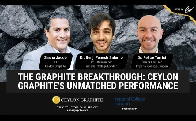
0:08 Thank you everyone for joining and welcome to the Ceylon Graphite Live Summit today hosted by 6. I'm pleased to introduce the speakers for today, Sasha Jacobs, CEO of Ceylon Graphite and Dr. Benji Fenik-Salerno, PhD researcher at Imperial College London. We will be expecting Felice Torriso, also a lecturer at the Imperial College of London. He should be joining us any minute now, but Sasha will introduce the 2 individuals and we will discuss their graphic, graphite and sensor research.
0:40 And after that we will be accepting questions. So as a reminder, you can submit questions in the bottom right hand side of the chat at any point during the presentation. As always, this summit is being recorded and will be available on Six.com in the coming days, so look out for that. I'll hand it over to you, Sach, to get things started, Bill. Great, great, thank you, Kyle. So I'm not going to speak too much today. I will leave it to the experts, Benji and Felice. As most of you know, we are a company that's not just focused on mining, we also have an incredible technical division based out of England and that is led by Dr. Sivabom and Dr. Malikabom, both are world-leading graphite experts.
1:26 Previously CTO at, you know, arguably one of the leading technical graphite companies that has a lot of products under development and IP and patents. And we similarly, as you may have seen, have filed several patents already and are continuously doing work on the technical side led by Siva and Malika. And Siva was also a fellow at Imperial College, still is a fellow at Imperial College, and through his extensive relationships and Malika's extensive relationships throughout the graphite and graphene world, They really know pretty much everybody that's in the business and have been able to secure a fantastic partnership with Benjy and Felice. We intend to make value-added products, some of which we've talked about before, some coatings and other products, and also looking at advancing the technology to ultimately make the anode material itself and the upgrading processes and technologies behind that to create a really competitive leading product amongst graphite anode materials and other applications, which we'll be talking about today.
2:38 So that's the basic overview. I had the great opportunity to meet Felice and his team a few weeks ago and learn, really walk through all the different applications that the team has been working on, which is tremendously exciting, and some incredible developments, and all using Ceylon graphite specifically. So I'll hand it over now to Felice, who leads the team. Both Felice and Benji are world-renowned experts in this field, in graphite and graphene and graphene applications. If you have a chance, if you just do a simple Google search, you'll see an incredible amount of work and interviews that the team has done and as I say are really world experts in this area.
3:24 So Felicia can I hand it over to you, I know you'll probably do an overview presentation of your work and the team and then Benji will talk about some of the specific exciting work that he's been doing after that? Yeah absolutely Sasha, well thank you very much first of all for inviting me to this webinar and actually giving us the opportunity to talk more about our graphene and 2D materials research in general, and then more specifically, the advantages that we obtained by using silon graphite in some key research areas that essentially enabled us to improve some of the performances in our devices. So let me start with a general presentation, a general overview.
4:15 Yeah, Felice, just in the center of the screen you'll see a rectangle with a share arrow. You can go ahead and share your screen and open up the panel. I can share, yeah, the screen. So you should be able to see the screen now yes and if you want to go into pretend view perfect now you're ready to rock and roll okay so well essentially this is a brief overview of the work we are doing with graphene and two-dimensional materials at Imperial College and specifically in my group which is the 2D web group, 2D materials and wearable electronics and biosensing.
5:02 And essentially we are based in South, in sorry, the Imperial College is based in South Kensington, we are based in White City which is actually a new development of Imperial College and particularly within this new area of a world-renowned University there is a research hub which has been established now back in 2019, it was right before the pandemic, with a key idea to realize the potential for major advances in chemical, molecular sciences and let me say also nanomaterials. And this is engraved actually in the statutes of the Molecular Sciences Research Hub. So essentially this is a state-of-the-art building with all the necessary facilities and labs to obtain breakthroughs in molecular sciences, nanomaterials and chemistry.
5:58 So within our group, We work a lot on, for example, advanced fibers and textiles. And in this case, actually, we used graphene primarily to create, for example, some types of fibers with specific layout. Here, for example, you can see a core shell fiber that uses graphene as the initial core for both mechanical reinforcement and electrical conductivity. And then it uses a combination of boron nitride, which is another material I'm going to talk about, and graphene as the external shell. So you can see this in a similar way to a coaxial fiber, but actually this is made at the microscopic level using nanomaterials. So we are looking at very, very small scale, essentially 10 to the minus 9 meters, which essentially means very, very small materials.
6:49 We're also using nanomaterials and particularly graphene to make, for example, smart and advanced polymer composite. And this was one of the first results that we've actually got with the with a silon graphite. Thanks to a collaboration by the Royal Society. I'm going to talk about more about it. This is just to give you an overview of the results we obtained with this material. In this case you can see ultra-stretchable conducting polymer composite. And more recently we've been working a lot on printed wearable electronics and also sensors. You'll hear more about it on a specific sensing area from Benji. And as an overview, we do quite a lot of work on printed electronics for flexible and wearable devices and graphene plays a big chunk of that power, plays a big role to essentially improve the conductivity of some of the interconnections and also integrate, for example, different devices, so interconnecting.
7:55 And then we also work on a more basic level on formulating a high quality graphene and two-dimensional material inks, starting from powder, from graphite itself, so graphite rocks itself, to creating inks and formulating them for different printing technologies. So essentially, we really start from the raw material in our group, and we are able to go down to specific applications. So we really build up all the different steps to go from the material to devices that could be directly incorporated, for example, in existing objects. In this case, for example, you can see a jacket sleeve. So we're actually integrating these electrodes into textiles. And of course, we care a lot about industrial compatibility. And so I'll focus a bit more about it as well. And to do that, of course, we need to produce large amounts of ink. So we are able to scale up the production process of 2D materials at the level of liters per hour if we wanted to. And then we're able to deposit it and coat it on different substrates, depending on the specific applications.
9:05 So as I said, we care a lot about the commercialization. And key factors for that are definitely cost and performance. So we want to have attractive and commercially available materials that lead to new products. Of course, these need to show better performance at lower cost, and that's exactly what we want to do. When you do that, when you develop that, manufacturability is extremely important. We also look at the figures of merit that indicate batch-to-batch reproducibility and also they lead to new technologies for example enabling new devices as I mentioned for example electronic textiles and wearable electronics is an entirely new field that requires new materials and can really open up to new devices and new applications.
9:57 And I would say, last but not least, mass production. So the upscalability of any production process for the materials that we make and for the devices that we then obtain afterwards. And this leads also to monitoring specific scaling factors. So if you want to keep the quality of course for every material and every device we need to identify what are the key scaling factors and we we really tend to do that. For example for the liquid phase exfoliation of graphite which is one of the I would say standard processes that uses a top-down approach to exfoliating graphene from graphite. In this case, it's a process that happens in liquid. Normally, you start from natural graphite and you exfoliate it in liquid. With the application of specific power, I'm not going to go into the details, but you can apply all sorts of power from ultrasounds to electrochemical power to, for example, shear forces and also microfluidic forces, you can actually obtain graphene dispersions that if they are tuned a little bit, they can really become graphene inks.
11:03 And there is really a quite extensive literature that can explain how to do this. And of course, when we did that the first time, we could reach few milliliters per hour with a small Bath Sonicator, for example, at that time. And then we worked a lot in improving the scalability of this and going from milliliters to actually liters per hour. So you can now really scale up and produce a lot of these inks in large quantities with a purity that is monitored. And this is monitored through specific scaling factors, as I said. So, for example, volume, the force you are applying, the initial concentration. So, essentially, without going too much into the details, you can see that we can scale, for example, the concentration with the amount of the initial concentration.
11:49 We can scale the output concentration with a volume of liters and we can scale the concentration with a force. So essentially by changing some of the parameters we can still control the concentration of our ink. So this means that going from 10 milliliters to 10 liters per hour doesn't compromise the quality of our graphene and this is very very important for scaling up. So this leads us to production of you know big bottles and a lot of material that you can really use for, for example, for devices and you can also share with collaborators. Just to give you an overview of what we're doing, for example, we don't just exfoliate graphene, we also work with other 2D materials. Maxine is, for example, an interesting family of 2D materials that is emerging recently.
12:39 Essentially the material is a compound made from for example transition metals with carbons or nitrogens and these early transition metals essentially combined with either carbon or nitrogen gives rise to different electronic properties. These 2D materials can be either conducting or semiconducting And you can see here on the right hand side, for example, some of the electron microscopy images. These really look like flakes in exactly the same way as graphene does. You see that lateral size of these flakes is averaged at 700 nanometers, so it's a bit less than a micron and the thickness is around 3 nanometers, it is peaked at 3 nanometers so it's something very very thin and large like platelets, exactly the same as what you get with graphene.
13:28 This is for example one of our typical graphene inks, definitely using silon graphite but also using any type of graphite available, you can obtain high quality graphene inks. Of course we'll show you how the silon graphite outperforms some of these, but you can still obtain dispersions with platelets similar to what I showed you earlier on, so 300 nanometers, 6 nanometers thicknesses. We also work with semiconducting 2D materials. MOS2 is one of the well-known ones giving high yield exfoliation, so concentration, and in this case you can of course get similar flakes as the other ones in the order of hundreds of nanometers with thicknesses of about 2 nanometers.
14:16 So again here we're looking at something which is very thin and large. So the aspect ratio for all these inks is very similar, however their electronic properties are different. You can imagine that the top 1 is more a conducting material, graphene is a semi-metal so it kind of stays in the middle. And then MOS2 is a semiconductor, so you can actually have similar properties, for example, to what you can obtain with silicon. Of course, not precisely. And you can see here that the shape of these is kind of similar. You know, They all look like flakes or platelets. So what do we do with it? The first thing we started to do is actually printing. So we take our graphene ink and we do a bit of printing. Here you can see, for example, an inkjet printer and a nozzle that is actually shown here. Let me just take the laser pointer.
15:04 So this is a nozzle of an inkjet printer. You can see a single droplet that is actually coming out of the nozzle. This is called drop-on-demand. So it's a technique with an inkjet printer that allows you to control precisely the volume for the material you're actually putting down. And with this you can actually print electrodes that are transparent and conducting on different substrates. Here you see a PET substrate. We print a transparent conducting graphene electrodes and on the right hand side for example you see a paper display using graphene electrodes as back electrodes so both of them are using graphene inks but you know they have very very different performance as you can see. So what is the advantage of going down to graphene? Why do you need to exfoliate graphite to get graphene? Well, I think this graph is a clear explanation and answer to this question. You see that without processing, So 0 exfoliation of graphite, you have a resistance, or what we call a sheet resistance, so a resistance per unit area, per square area, of around 80 ohms, slightly below 80 ohms per square. If you take the same graphite and you do some exfoliation processing to obtain graphene, you see that this resistance drops to a very, very low value, below 10 ohms per square. So it goes down by essentially 1 order of magnitude from 80 to 8, or actually 2 orders of magnitude, 0.8
16:35 on per square of 25 microns thicknesses of the printed film. So this means that we have a gain of 2 orders of magnitude in conductivity, which means a reduction of resistivity. So the exfoliation is needed because graphene, overall, has actually a better thin film conductivity than what you can normally get with graphite flakes. And this is not to say that the single flake is better, but the printed film is better because, essentially, you have a better connection between these flakes and you facilitate hopping of charges from 1 flake to the other. So what do we do with it? One of the easiest applications that we started to do doing ages ago now, it's actually screen printing of graphene ink. Screen printing is a very popular technique in industry, for example to make leaflets or brochures.
17:22 Essentially it's based on a squeegee, which is a kind of brush, and this brush pushes the ink through a screen that then deposits the ink on a substrate with a specific pattern. So in this case, we collaborated with a company that was actually doing active smart posters. And at that time, they were using carbon pads, standard carbon electrodes, and silver inks. These are silver inks trucks. Now, silver is very, very expensive. So to get that conductivity, they were spending around 2,000 pounds a litre for that ink so it's a lot of money to get these posters and those posters were incredibly expensive and they couldn't really sell them. So what we actually did, we designed the same poster, but we used entirely graphene ink.
18:09 And screen printing graphene ink is overall much cheaper than printing silver, as you can imagine. And therefore we could essentially obtain exactly the same properties of the silvering, because they actually didn't really need it, the true conductivity of the silver, but lowering substantially the cost of these posters. And then we could incorporate, for example, these as a motherboard over here, and then we could overlay this nice pattern. And you can see here that this is, for example, a poster that hopefully, if the video starts, it's not starting here for some reason. Let's see if we can get it out. Yeah. Hopefully you can see this. I hope you can hear the sound, but essentially this is a smart poster entirely using graphene ink and it works.
19:05 Of course, we wanted to be a bit more advanced than just doing smart posters, so with the graphene ink we started printing RFID tags. RFID antennas normally are very popular, for example, in smart cards or badges, as you know, and currently they're made of copper or silver. So here you can see for example a paper that we published using graphene ink. This is screen printed graphene ink and here you can see actually
19:30 the antenna RF pattern all around it with a very nice advanced compared to standard RFID tags, so commercial graphene RFID tags using ultra high frequency for these graphene antennas, we reached after a reading distance of up to 11 meters, exactly the same frequency you normally operate RFID tags. And then of course, we started collaborating with a Royal Society Industry Fellow, Dr. Siva Bom, who is now part of Ceylon Graphite. And with using Ceylon Graphite to make our graphene ink, we actually developed a highly stretchable and conducting graphene ink that can be printed. So essentially, you can imagine that this ink can be screen printed, or even now we are trying to develop an inkjet printing version of it, that then dries and can be easily stretched out. So this is extremely important when you want to do stretchable and flexible electronics.
20:38 So having stretchable electrodes enables to actually stretch out in a specific direction your device without compromising the electronic properties. So here for example you can see an elongation of 60% of these electrodes keeping a conductivity of around 500 Siemens per meter which is a standard conductivity you would normally get from carbon parts. So this really opened our eyes on the potential of xenon graphite and developing specific advanced polymer composites. So then we move forward towards wearable electronics. And when I talk about wearable electronics, I'm sure you know a lot about the wearables nowadays, but if you think about all these wearables Most of them they look like watches, you know They look our Fitbit or or Apple watch and these are all made of mostly Rigid electronic components that are just interconnected, you know, sensors that are rigid, transistors, LEDs that are rigid. Neither of these are breathable nor stretchable.
21:39 So if you really want to enable wearable and stretchable devices, you need to go towards breathable and stretchable electrodes. And one of the first works we did was actually using a textile that is embedded into a graphene coating, graphene pad. And in this case, we actually used this graphene pad to replace the standard silver chloride electrodes for ECG. These are normally rigid electrodes that are put in the body to monitor the electrocardiogram. And as you can see here, a comparison of the silver chloride standard electrodes with a graphene textile electrode gives exactly the same pattern of the so-called PQRST peaks typical of the heart rate. So essentially you can replace a rigid electrode with a graphene textile breathable electrode you get exactly the same signal with a difference that this can be easily incorporated into a t-shirt or a piece of textile.
22:38 And of course it's stretchable, unlike the rigid metal, it's biocompatible and washable. And on top of it, it also has a very low power consumption, which is very important for wearable devices. Then we also like to do printing, as I said. So for example, we started inject printing graphene oxide, which is a chemically modified graphene. And when we print these on textile, for example, you can see a graphene coating on top of this textile. You can see that there is a color change here. And then with some heating, around 120 degrees heating, you can see that you can form a nice coating on top of the textile. Now this coating, if properly engineered, can actually lead to very nice sensors. So here you can see for example a graphene strain motion sensor. This is a piece of cotton coated with graphene and it achieves actually a very nice change in resistance linked to the bending of the piece of textile and this is simply because we're engineering very well the coating on top of the textile. For example here you can see that when you stretch this piece of textile down or up, you can actually monitor the change in resistance. You see there is a substantial change in resistance. And then this change in resistance can be easily linked up to the wrist up position or the wrist down position. And then we are incorporating this, of course, for example, in clothes to monitor pressure and motion. And this, of course, can be easily
24:09 already integrated as a patch on commercial devices. And that's the actual piece of textile that is operating up and down. And we also demonstrated that device can be washed up to 20 times without compromising the properties that much. Then we went a bit farther, we actually fully inkjet printed electronic circuits And when you want to do electronic circuits, you need to start from the first device, which is very important. It's actually a key element of the electronic nowadays. And that's the TFT, the thin film transistor. Essentially, we are printing transistors on textile using graphene and other 2D materials. So here you see the textile substrate and then the graphene channel of the transistor.
24:57 And then these are the 3 terminals, gate, source and drain. Essentially, these are 3 metal contacts that we are contacting to modulate, to change the current in our device. And this is the typical switching behavior of a transistor, if you know what it looks like. If you don't know, then believe me, this is the typical modulation of a graphene transistor, and essentially you can switch the current on and off. And the nice thing is that the speed of the electrons, so the mobility of these electrons on a specific voltage is extremely high compared, for example, to standard conducting polymers and even semiconducting materials that can be injured printed at the moment. It's around 1 order of magnitude higher with a low power consumption. And then of course we got excited and we just don't want to print a single transistor.
25:42 So we actually printed circuits. So just imagine a piece of textile, no rigid wafer, no silicone, nothing, just textile, with printed graphene on top, and this textile becomes an element, for example, of a microprocessor, like an Intel microprocessor, but simply on a textile. So what we did here, we developed, for example, a 2 transistor device where we can switch on and off the system depending on the input. We get an inverter, so an inversion of the signal. So this is the input, positive, negative, and the output is negative, positive. So we're actually inverting the signal. And then we challenge ourselves and we actually went to do a 2-bit reprogrammable memory cell. So again, a piece of textile which now becomes a memory, 2-bit memory, without any rigid electronics.
26:31 So graphene really enabled us to unleash the potential of these 2D materials for actually wearable electronics and electronic textiles. Of course, it's not just electronics. One of the successful impacts that we had using, for example, EPSRC funding through this impact acceleration account funded by Imperial College is actually to demonstrate that we can transfer graphene ink on textile to make, for example, thermally conducting coatings and heaters. So in this case, you can see that we can control the temperature of a specific graphene pattern that we deposit on textile simply applying voltage. So by applying voltage, we can make a heater localized in specific areas of a t-shirt. In this case, this is a base layer for cyclists.
27:19 For those who are cycling they would know this very well and so for example you can make sure that the chest is at a specific temperature which is very important for example when you're cycling at very low temperatures. And other applications are, for example, large-scale and rapid low-cost chemical sensing. You hear more about this from Benji, so we'll go very, very quickly. Just attend Benji's talk after mine. But essentially, here we developed a sensor, an electrochemical sensor based on graphene. In this case, you can see we are at a very advanced stage here. We developed a PCB board with a specific graphene sensing, and thanks to the graphene, the xylon graphite here, we could actually outperform other existing printed GFETs that are currently out there. And we could obtain a high concentration for these graphenings.
28:08 Now, the advantage is that, first of all, we could actually do a specific recognition and detection of antibiotics, thanks to this graphene channel with a limit of detection of around 50 micromolar, we can even go lower than that, and we can also do heavy ion detection, for example using a specific ion selective layer or ion selective coating that you can put on top of the graphene and this allows you to detect down to 5 micromolar of specific ions. So this really goes to the bottom, the limit of detection that we have at the moment, so it really challenges current devices. And one of the last applications is of course going beyond graphene. As I said, we can develop inks made by other two-dimensional materials, and these are for example other metal oxides or metal tichalcogenides, and even boron nitride, which is essentially a complementary element to graphene. It's still hexagonal but it's actually a wide bandgap semiconductor, essentially it's an insulator, and we can print these devices. Here you
29:15 can see again a single droplet which is actually coming out of an injured printing nozzle, simple drop-on-demand, and by controlling this printing we can actually fully print electronics using two-dimensional materials. Here you can see actually a schematic of the type of circuits. So I don't want to go into the details of the circuits. I just want to show you here, between the 2 electrodes, source and drain, which are typical of a transistor, you can see the flakes. These are MOS2 flakes that are bridging, for example, so they are connecting the 2 electrodes, and these flakes are actually modulating the current. You see that current can change by orders of magnitude. Here it can go up to 2 orders of magnitude higher current than in the off state. So essentially, this on-off modulation is typical of a transistor.
30:05 And here we are showing that we have the typical output curves of transistor simply by fully printing MOS2. And then by combining many of these transistors together, you can see here 2 transistors that are interconnected, you can actually make fully 2D materials based integrated circuits. So these 2D materials can now in a solution processed way, so in an ink form, can really unleash the potential of 2D materials for printed electronics. And in some cases, they can become complementary to organic electronics, which is currently used. So in conclusion, I just want to tell you that we can really work with a lot of 2D material inks. And we have demonstrated in our group that these are a viable platform for printed wearables and even e-textile electronics.
30:53 You can make a lot of electronic textile circuits using graphene and the other 2D materials, and also the platform of 2D materials really generates a new range of high performance integrated circuits that can't really be achieved by, for example, any other printable dispersion or printable ink at the moment. And as you'll hear from the next talk, graphene field effect transistors actually can enable large-scale and low-cost platforms that could be used for diagnostic sensing or even commercial circuit boards in the future. And of course I want to acknowledge all the funding that made this possible, from fundings at Cambridge when I was early on, then to funding at Imperial, ERC, EPSRC, and of course the Isaac Newton and the Graphene flagship.
31:45 And this image is a quick overview of what we do at Imperial College at the moment, going from flexible electronics to actually sensing smart packaging, and also more fundamental studies on the electronic transport and the nonlinear optical properties. And I think with this, I can stop. Thank you. Thank you, Felice. So you can go ahead and stop sharing your screen as Benji starts to share his screen. And I'll just address a couple of the questions in the audience, if you don't mind. Can any part of the technology itself or any specific applications be patented? Well absolutely, I mean we already have around 5 patents on this technology and we have another couple of patent applications, so definitely there is a huge potential for patenting this. Of course, the graphene field itself is populated by a lot of patent applications already in specific fields. But there are other fields that haven't benefited
32:51 from actually graphene material per se, and with some of the key performances that we are achieving now thanks for example to materials like xylon graphite, can, I would say, can be now enabled? So essentially areas that couldn't be enabled earlier on, they could be enabled now, so we potentially could patent in areas that were forbidden before, I would say. Thank you. And Rock had a question as well. Some companies are developing graphene using acetylene, actylene, no, sorry. Acetylene. Thank you. And a combustible method. How does the graphene compare to the graphene prepared using graphite?
33:41 How does the graphene prepared, I think, with acetylene compares to the one prepared?
33:46 Yes. Well, there are very different synthesis methods. So the, I think the one that I'm talking about is actually a synthesis starting, it's a chemical synthesis essentially. So ours is more, it's called liquid phase, but essentially it's a mechanical synthesis. You start from graphite rocks and essentially pulls out flakes out of that. So I think the difference is in what you obtain at the end. So in our case, essentially you obtain a distribution of flakes in a dispersion. These are normally called few layers graphene. You have a population of monolayers, so purely graphene flakes, but also you have a population of multilayers. And this has some advantages and disadvantages. One of the advantage is actually you can still average the overall behavior of these materials and we have demonstrated that this is very similar to the essentially chemically synthesized graphene.
34:41 So even though you have multi layers, for example the field effect transistors that we obtained, they still have the Dirac modulation. So the typical ambipolar behavior of graphene. This means that you can go down with a much cheaper route than synthesizing by acetylene, obtaining very similar properties. Of course, acetylene per seminal, acetylene based on chemical synthesis in general, gives you a more, I would say a purer monolayer because of course most of the cases you actually have 99% monolayer with of course a polycrystalline behavior. However, that synthesis route normally doesn't allow you to have printable inks. So the entire field of printed electronics, wearable electronics and composites is kind of forbidden because you can't really make inks with a high concentration.
35:34 You rather use for example chemical synthesis to make perfect single layers for for example specific applications like optoelectronics that require monolayers 100% monolayers or for example displays or coatings where you actually need a 100% monolayer coating. So I would say that the exfoliation, the liquid phase exfoliation addresses mostly the need of printed wearable and composites by with particularly with the silon graphite with high quality graphite sources or raw materials really but by almost matching the same properties that you would obtain with high quality chemical synthesis, but with the advantages that you can still print the material.
36:24 OK, thank you. We better get to Benji's presentation. There are questions coming in, And that's great, but we will leave them till the end. So Benji, why don't you go ahead and share your screen and we can listen to your presentation. Okay, so thank you. So I'll just be giving a very brief presentation about the work that I've been focusing on over the last 3 to 4 years now, which was developing a sprayed graphene lab on PCB platform for multi-analyte detection. And so to put everything into context, I'd like to introduce to you our patient for today, Chantelle. Now, Chantelle isn't feeling very well, and as a result of that, she needs to access some kind of routine health care testing. This could be for screening or just because she may be sick at the time. In any case, what she does is that she
37:18 contacts her local healthcare practitioners, makes an appointment, and then visits a clinic where a sample is then taken from her to be tested later on. And then that sample is typically transported to a hospital or clinic where it is further analysed. And so that's where the tests are actually carried out. And Chantal can expect to wait anywhere between 1 day to several weeks for her results to actually make their way back to her and her healthcare team. And then she can then discuss with them on what the next steps could be and as you can imagine this is actually quite a complicated system with many moving parts and as a result of that also comes with quite substantial costs so what we've seen over the last few decades or so is this push to move away from the centralized testing system to a more decentralized testing system and the fact these tests these decentralized tests can be described using the reassured criteria which essentially state that these tests should be effective, they should be low cost, and they should be carried out close to the end user.
38:25 And already a number of these tests already on the market, the most famous being the glucose monitor, and the LFT tests, such as the ones used during the pandemic or the pregnancy tests which have been around for a couple of decades now. But it's still very much early days and there's still a lot of work to actually bring about more of these tests closer to the end user, so closer to the patient, for the patient themselves to actually use, or for their healthcare team, let's say their GPs, to use during routine visits to their clinics. Now, as Felicia spoke about during the last 30 minutes or so, we are a team that's focused on nanomaterials and mainly graphene is one of the things that we excel at and making inks and so when I started off my PhD in the group what we set out to do is to take the very best advances in nanomaterial science from the last decade and a half and combine it with existing manufacturing techniques to create a sensing platform which is low cost, which can detect for multiple analytes, and which is scalable using today's technology.
39:33 And in the next few slides, I'm going to be going through that journey of how we produced our INGO sensing platform. Now obviously, Pletcher is already interested in introduced graphene. It's a wonderful material. It has really some amazing properties. But from our perspective, from the chemosensing side, what we really care about is that it has a high mobility, which allows us to use it in electrochemical sensing. It is a stable material, so once you produce it, you don't really have to do much you can you can deposit it and then you can leave it out in there you know you not need special packaging conditions. It has versatile functionalization which means that we can attach things to the surface of this material that allows us to detect for different things specifically.
40:20 It is abundant, so we produce our material using graphite, ceylon graphite for example, and that is an abundant material that we can produce and that we can source in large quantities. It can be made using promising biocompatible routes, which means that we can make it in environmentally friendly ways and we can also make it in ways that it can be used for, let's say, electronic textiles. And importantly, it is solution processable. So that means that we can produce inks out of graphite to produce graphene that we can then deposit using printing or spraying. Now the way that we produce our inks is a process known as liquid phase exfoliation. So the way this works is that we start with our container, we add to it a dispersant and some stabilizing agent, let's say some kind of surfactant, and we add to that our bulk layered material, so in this case graphite.
41:16 And then what we do is that we apply a mechanical force to our dispersion. So what we're doing here is a process known as sonication. So we're creating bubbles in our solution and when these bubbles collapse they release a tremendous amount of energy. And what happens is that we have graphite, which is essentially many layers of graphene stacked on top of each other. And this release of energy causes these layers to push apart. So we go from bulk-layered material to many layers, to few layers, down to single layers. And we end up with a population of these flakes within our mixture and so after a couple of hours of sonication we then carry out a centrifugation which means we spin this at a high velocity and then we take the liquid from the top and that is our 2D material ink.
42:10 Now once we've produced our 2D material ink, our graphene ink, there are a bunch of different techniques that we use to actually measure how well our production has worked out. But I would say the most basic and one of the most important actually is identifying what's the concentration of our ink. And so we use techniques such as UV spectroscopy to carry this out. And now the way that we produce our ink is with a stabilizer on a SPVP. And this has been known to literature for a number of years, but we really worked hard to optimize this. And actually, by using the C-long graphite, we actually discovered that we could improve on the previous best in class inks. And actually, we can see somewhere around the threefold improvement in the concentration.
42:58 I really can't emphasize how enabling this was to our work, because what this allowed us to do is allowed us to fabricate our devices in less time and with less deposition passes. And usually what happens is that the more deposition passes you have, the more difficult it is to produce high quality devices. So fewer deposition passes enabled by higher concentrations actually allowed us to improve the performance of our device. And then we also carry out other characterization techniques. One other one would be a technique known as atomic force microscopy and what we're doing here is we're actually looking at what these flakes look like. So we're looking at the lateral flake size and the thickness of our flakes And in the inks that we use for our device, we can see that we have a mean lateral flake size of around 200 nanometers and a mean thickness of around 6 flakes.
43:57 So once we have our graphing ink, then The next question is what do we do with it? So what we did is that we designed actually an architecture using a printed circuit boards that allows us to manufacture the base of our device really in high quantities at very low cost. So even at the laboratory stage, we're talking less than $1 per device. And then once we have that in place, we spray coat, we deposit our graphene on our active area. So that is the black region on the image shown on the screen. And sometimes, in some cases, depending on what we're detecting for, we can also deposit a selective layer on top of that graphene layer. And once we've done this, we're ready to actually start operating our device.
44:47 Now, the device that we're operating is known as electrolyte gated field effect transistor. I won't go into the dynamics of how it works, but essentially when we operate it, when we're changing the voltage of the gates of our device, this is the current flowing through our graphene. So we get this characteristic U-shape flowing through the graphene, which is our active sensing layer. Now what we can observe is that when we change the solution of the analyte on top of our sensor. So essentially we're dipping our sensor in a solution. By changing the pH, we can observe that at lower pH, we see a shift to the left. At higher pHs, we see a shift to the right. And if we do that at a couple of other different pH values, we can actually do a calibration curve and observe that we have a linear behavior. And what that allows us to do is to actually use our device to measure for differences in pH. Now pH is a very important analyte to detect for both in biology and in industry.
45:55 In biology for example it can be combined with certain enzymes such as penicillin which Felicia spoke about briefly and you can actually use it to detect for the quantity of the antibiotic penicillin in a patient's, let's say, blood sample. And so by measuring the pH combined with an enzyme, you can actually measure how well the patient is breaking down the penicillin and when to actually add more for them to take the next dose. So this is what the device looks like when it's operating, when we're sweeping the actual gate voltage. But what we can actually do is that rather than operating at a series of different voltages, we can actually operate at a single gate voltage. So you can see, let's say, operating at minus 200 millivolts, we can observe that the current flowing through the graphene is proportional to the pH of the solution that we're detecting for.
46:51 And so this is what it looks like in real time. So we're making very small pH changes, 0.4 pH units, and what you can observe is that we're getting these repeatable, quantifiable changes in the current flowing through our graphene sensor. And the response time is less than 20 seconds, can work in a range of pH 3 to pH 11. And as I said before, the cost of our device is less than 1 dollar per device. Then 1 further application of our platform, so this is essentially the same platform that I have just spoken about, but by simply depositing an additional layer on top of our sensor area, so the black area over here that is our graphene deposition. By depositing an additional membrane on top of that, we can actually detect for other species. So in this case, this is the ion selective GFAT that we have worked upon. And so this is a complex membrane on top of that. But the key entity here is the ionophore.
47:57 So what this molecule does, it actually allows certain ions to make their way through the membrane and towards the surface of the sensor, whilst other ions are excluded out. So this only allows a certain type of ion to make its way to the surface, and that in part causes a change in the electrical properties of our device. And so this is what it looks like. So we're operating it as we described previously, the exact same device, but just with the addition of the ion-selective membrane. And you can observe that in this case, detecting for sodium, so we added an ionophore specifically for sodium, we see these proportional changes in the drain current and the current flowing through the graphene channel. And when we plot these out, we can actually observe that there is a range within which our performance is linear, which again means that within that range we can actually produce calibration curves and that allows us to quantify, in this case, the amount of sodium in our sample. And I would say the key takeaway here is that by simply changing the composition of the membrane on top, we can shift our sensing away from sodium and to other types of ions, let's say potassium, calcium, heavy metals such as lead or mercury, and even some anions such as fluoride.
49:17 All of immense biological importance, both in environmental sciences as well as in medical sciences. And yes, that brings me to the end of my presentation. Thank you for listening. I'm very happy to discuss any questions that you may have. Thank you. So this is a reminder you can submit questions in the bottom right hand side of your screen. We still have some questions here so let's get into them. Tim asked about these applications are they capable of being purposed towards 3D printing? What's the scope for commercialization here? I think I can answer that, maybe.
50:07 Right, so 3D printing, of course, is a very different technology than 2D printing that I've described in my presentation. Specifically, if you're looking for 3D printed devices, the type of composite that you need to develop normally, it depends on which 3D printing technique you're using, but definitely needs to have some specific properties that are, for example, having thermoplastic properties that you can, for example, use in in fused deposition modeling 3D printing, or, for example, some curing properties that you have in SLA type of techniques. So in this case we have worked quite extensively in creating extrudable composites.
51:00 So at the moment we have a couple of projects where we are embedding high concentration, few layers graphene or few layers platelets of these originally layered materials. I wouldn't really call them 2D materials because in the case of 3D printing, the concentration of materials that you need to achieve is extremely high. And therefore, the only way really to get there is to try and use a liquid phase exfoliation process that gives you mono and few layers graphene or few layers 2D material, few layers layer materials all together so that you can increase the concentration to maybe hundreds of milligrams per milliliter or even more than that. And so that you can have actually enough material to then 3D print a deposit is into a kind of fiber shape. For example, if we're looking at fused deposition modeling.
52:00 So to do that, you can definitely increase the concentration of these materials and achieve 2 main properties, actually 3 main properties. The first one is mechanical reinforcement. This has been extensively demonstrated already. So you can reinforce, for example, resins or our typical thermoplastic polymers like, for example, PLA and ABS, which are currently used in 3D printing technology, by introducing graphene and any carbon-based materials, even carbon nanotubes. The big difference though with introducing graphene is that you can also improve the electrical and thermal conductivities. So you can make your extruded or printed polymer composite not only electrically conducting, so for example you can use it for printing interconnections in circuits, but you can also dissipate heat.
52:57 And now this becomes extremely relevant for example in packaging in electronics because you could 3D print packaging that are already themselves dissipating some of the heat generated by microprocessors. Or, for example, you can use these composites as 3D printable thermally conducting paste to dissipate heat. And they can also be relevant in other areas, for example in the oil industry to dissipate heat in pipes or for example in wearable electronics to harvest heat from the body. So there is an entire field actually that is really caring about this. So in terms of commercialization actually there are already examples of commercial products using 3D printable graphene based things. I think the big difference and the winning nice spot there is being able to demonstrate that these composites, 3D printable polymer composites, have really an added value compared not only just in terms of cost, but in terms of performances, compared to other types of 3D printable composites using, for example, metal nanoparticles or semiconducting or conducting nanoparticles.
54:12 And I think one of the big advantages is precisely in the thermal field, because graphene has the highest ever thermal conductivity you can find in a material, and other 2D materials like boron nitride can combine a very similar, slightly lower, high thermal conductivity, together with electrical insulation, which is actually a very unique combination. Normally, thermally conducting materials are also electrically conducting, So being able to decouple these 2 properties is quite unique. So I think there is a very interesting scope for graphene and boron nitride in 3D printing, but it has to be precisely tailored and that's I think the direction the industry should go to.
55:04 Thank you. I'll follow up with that with PS Vets 8 question here. In the beginning application with coaxial structure, does the boron nitride serve as an insulating material? Correct. So the idea of creating this coaxial structure, of course, is trying to create a microscopic version, or in this case, the total diameter of the fiber, I think, is around 100 microns. So definitely each layer actually is hundreds of nanometers or a few microns. So microscopic structure of a macroscopic coaxial cable. So we go from coaxial cables that are normally in the order of millimeters down to microns. Okay, so these become really fibers.
55:51 And yes, the 2 graphene electrodes there are serving as electrically conducting layers. Actually, 1 is core, the other one is a shell. And then the intermediate boron nitride shell is a dielectric layer or an insulating, yes, layer that has a specific dielectric function or dielectric constant that allows to insulate and separate the 2 layers and yet storing energy or storing charge in this specific case. So for example you can imagine you can create a capacitor, a cylindrical capacitor.
56:36 So you can have a capacitance per unit length. And this is very, again, it's important because it enables you to store charge on a fiber. So if you can weave then this fiber into a piece of textile, you can actually store energy or charge locally. So this is very important for wearable sensing because you could power sensors on site directly without having to put a battery at the moment. And as you can imagine, one of the biggest hurdles in wearable electronics is actually how to power these devices. So at the moment, battery is the answer. So if you can get away Without batteries, that's a very good area. Great. Now, as C-Log Graphic has put together this event and there are shareholders listening, there are some questions more directed toward you, Sasha, that I will be asking here.
57:31 First is Gary's. Stock action is very muted. Why isn't all this good news generated any excitement in the stock price? Well, I think there's a couple of things. I mean, the first is, as most shareholders know, we've had quite a few delays on the production commencement, so we're hoping to overcome that here shortly and get the full-scale commercial production going. So I think that's one of the things that people have been waiting for that. I do agree, I don't think we've had enough emphasis on the technology aspects that we're talking about today, absolutely. I think that's something that we intend to do more and we will have a dedicated website of the Holyland subsidiary in the UK that's doing all of this work, where we can talk much more specifically about all the different things that we have released in the past, but we'll have a dedicated site to that, hopefully have that up in about 8 weeks.
58:29 So That's the intention there. I see another question I can just go right into as well, but also Felicia and Benji might have other things to add to that. The question was, can Ceylon Graphite be used for anodes, EV anodes, and the answer is absolutely. Not only can it be used for anodes, it has... If you go to our website, salongraphite.com, you'll see under the news section, I think it was in... Earlier this year, I think it was in February, you'll see work done also some by Imperial College and other institutions that have extensively tested the material and shown that it outperforms any other graphite material in batteries, including synthetic graphite. So the answer is, yeah, absolutely. And that is our intention.
59:19 As we've mentioned before, our intention on the battery side of things is to upgrade NC anode-ready material, and we're finalizing working on discussions with partners there on the offtake side and OEM side, but it looks like that will likely be for the battery – will likely be upgrading in the US for that. Felicia and Benji, I'm sure you've got – we've got lots of questions coming in here, but in terms of graphite and anodes and our specific limiters, is there anything else you wanted to add there? Oh definitely, I mean we haven't ourselves tried to make anodes for EVs at the moment, because that's an area that I know you guys have covered already through other works. But in any case, I mean, looking at the conductivity that we obtain for our devices using silon graphite, conductivity and stability of these electrodes. I mean, we are also using your graphite, xenon graphite as an electrode in a different configuration.
1:00:27 So if it works, in our case, giving that stability and that conductivity that enables us to carry the current that Benji showed in our device, definitely it should show excellent performance in anodes, so in electrodes in general and specifically anodes for EVs. So despite we didn't try it ourselves I definitely can't see any reason why it shouldn't show very good performances. Gentlemen do we have a hard stop in 2 minutes here or can we ask a couple more questions? If the hard stuff happens. But Leech and Benji do you have a few more minutes? Yeah I can do a few more minutes.
1:01:13 Yep me too. Okay some great some great questions coming in here. There's another one. So there's a question here that's directed to me, so I'll just jump in really quickly about the volume for these applications versus traditional graphite applications in particular batteries. Yes, the volumes are much lower for now. Obviously, everybody, and Felicia and Benji can talk much better about this than I can, but the potential for graphene and graphene products is huge. But in general, in terms of the volume overall that's being used for batteries, you know, will be smaller. Having said that, our goal here is to be in the value-added material space, not just sell the graphite, but have IP collaborations, as we're doing with Imperial College, and partnerships where we're getting that value at a margin, because the margins on these products are of course very, very high.
1:02:12 And there is IP protection around them, which provides a significant competitive advantage. So, they're very much 2 different products. Volumes are less, but the margins could potentially be a lot higher. Kyle, did you want to read out some of the other ones that are more directed towards? Yeah, I can read out some for sure. M. Bester is asking what steps need to be completed to begin commercial production? Well, it depends commercial production of what. I mean, the C-long graphite could be, of course, a product itself. But if you want to make, if you want to go up the value chain, for example, start producing inks, for example, or the devices that we've shown, I think the important points are the ones that I've mentioned at the beginning. So the batch-to-batch reproducibility, scalability, and mass production, as well as improved performances compared to the existing devices. So the last one we already shown, we already shown that we can do improved performances.
1:03:26 So we know that the device is worth, let's say, investigating. Scale-up production, there are routes for scaling up production. So the only step that in our, I would say, in the application that we have shown today, we need to really assess is the batch-to-batch reproducibility. So we have done, I would say, a relatively limited testing, designing few devices in the order of tens of these sensors and the variability of the performances of these sensors actually is very low. So we don't get, I think Benji correct me, I don't remember if it was 10% or 5% Yes, it's plus minus 7% Plus minus 7% of variation of these devices Of course, to commercialize this you need to investigate a very big number of devices to make sure that you minimize the variation, the variability, and so you reduce essentially the distribution of performances.
1:04:31 However, the devices themselves at the lab level, they essentially perform in a very similar way. And I think this is maybe the missing step for our technology. I think maybe in terms of the material process, Sasha can comment a bit more about whether this can be scaled up in a different way. Yeah I mean our goal is is entirely commercialization of course so you know extremely excited by this collaboration with with Fletcher's team in Imperial College because our goal is commercialization. So it's what applications are the most demand, where such as the sensing device, where does our performance, our material, sorry, provide a significant competitive advantage. And that's really what's so exciting about this news and these results on Benji's work, but also others of the team that I was able to hear from similar results for a wide range of applications that we've been outperforming.
1:05:31 As I said, we've outperformed on the batteries themselves as well. I'll jump just in another question there's lots of questions here I don't think we'll be able to get to all of them but of course we can answer more by by email. I'll just really quickly answer 1 about the anode for anode material the conversion rates. So as you know we're starting with a 95% plus carbon which is a massive advantage there so we don't you know we don't have huge primary processing required. We're coming out at 95% carbon first and then to get to the end of material we have a smaller step to to get there. So our conversion rates are you know are much better than other flake but it performs and as I said it outperforms other flake material so it's it's a better conversion rate and the cost, the question about the cost again because there's no primary processing and because you're taking a 95% to 99.95 that is a much lower cost in terms of processing that than a precursor of say 80% that others might be using.
1:06:43 There's some more technical questions that would be, while we have Felicia and Benji, I know we don't want to keep you too long. Kyle, can you see the other ones I missed? Oh, there's 1 from Tim about, could you perhaps speak to methane cracking and chromatography derivations of graphene and how these compare with the liquid phase exfoliation methods that that you're using with our material? Okay, So what's the first part of the question? Chromatography? Yeah, it says, could you perhaps speak to methane cracking and chromatography derivations? Well, I'm not an expert in chromatography derivations, so I don't know, but definitely from methane cracking, as I said, the 2 techniques are very different. So methane cracking normally can be deposited I mean the graphene from methane cracking can be normally deposited by creating a a by nebulizing essentially this into a gas and then forming this kind of graphene flowers, they call it graphene flakes that are crumbled a little bit in a gas phase and then solidifying as the gas cools down.
1:08:09 And normally, this allows to have very, you know, very good, still very, very high concentration and the synthesis is done in powder form. So essentially this process doesn't go through the graphite to graphene process that we are doing in Ceylon graphite. So as I said previously for the chemical synthesis, I think the comparison is similar. In this case, you directly go into a graphene-like material, starting from methane, so from a gas phase, that though doesn't have the distribution of mono-multilayers, that in some cases actually is beneficial and the other thing is that normally you you end up with a powder that has already I wouldn't say crumbled but definitely deformed graphene while in our case particularly when you do liquid phase exfoliation, the graphene flakes tend to be more intact.
1:09:09 So they tend to, you know, retain the original, I mean, as I show you in the electron microscope images, these really look like platelets with very sharp edges and very large sizes. Normally the synthesis done from methane cracking, for example, tends to give you this crumbled graphene. Now for some applications this gives you a higher surface area. So for example, for electrodes in supercapacitors, actually it could be an advantage, but in some other areas, like the ones we are doing, you don't want to really have something which is crumbled. You don't, we don't really need high surface area. We just need very good electronic properties. And very good electronic properties means high quality graphene. So essentially, if we are linking up these 2 things, high quality graphene enables us to have such properties.
1:10:01 And as a consequence of that, perhaps silica graphite is a very high quality material. Of course, as I said, it depends on the applications. Every application has different requirements. So some areas you may compromise on the quality, but you rather increase another parameter, which could be the surface area, for example. Thank you. Just recognizing that we're over time, what I would suggest is some other great questions that we weren't able to get to, and if there's any others, please email us at info at salemgraphite.com, and if we can't answer them, then I'll be emailing Felice and his team to get the answers, and we can address any questions we didn't get to or any others as well.
1:10:52 Most definitely. Thank you for the time gentlemen and the presentations. Obviously a well engaged audience here too. So Thank you for all of the attendees. Sasha, if you have any closing remarks or any other news, please feel free. Well, first of all, of course, definitely wanted to thank Benji and Felicia for all of their time today. But more than that, thank you and your team for the incredible collaboration that we have between Sodium Graphite and your team. It's tremendously exciting, and I think we're able to share now over the last hour what we're planning to do in a way, you know, tangibly with some great presentations, we're able to demonstrate, you know, what the plans are here for our collaboration going forward and some potential commercialization, and very excited by it. Thank you so much for your partnership and for your time today.