SUSS MicroTec SE · XETR:SMHN
SUSS MicroTec — Investor Presentation (May 2011)
39 slides from SUSS MicroTec's investor presentation, May 2011
Slide 1: Company Presentation May 2011
Company Presentation Company Presentation February May2011 2011
Slide 2: Disclaimer
Disclaimer This presentation contains forward-looking statements relating to the business, financial performance and earnings of SUSS MicroTec AG and its subsidiaries and associates. Forward-looking statements are based on current plans, estimates, projections and expectations and are therefore subj
Slide 3: Content
Content I. Executive Summary II. Products and Markets III. Growth Opportunities IV. Financials V. Outlook VI. Appendix 2
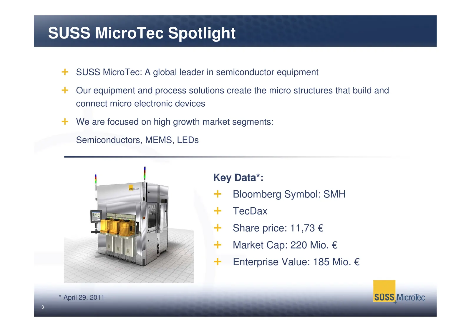
Slide 4: SUSS MicroTec Spotlight
SUSS MicroTec Spotlight SUSS MicroTec: A global leader in semiconductor equipment Our equipment and process solutions create the micro structures that build and connect micro electronic devices We are focused on high growth market segments: Semiconductors, MEMS, LEDs Key Data*: Bloomberg Symbol: SMH
Slide 5: SUSS MicroTec Key Information
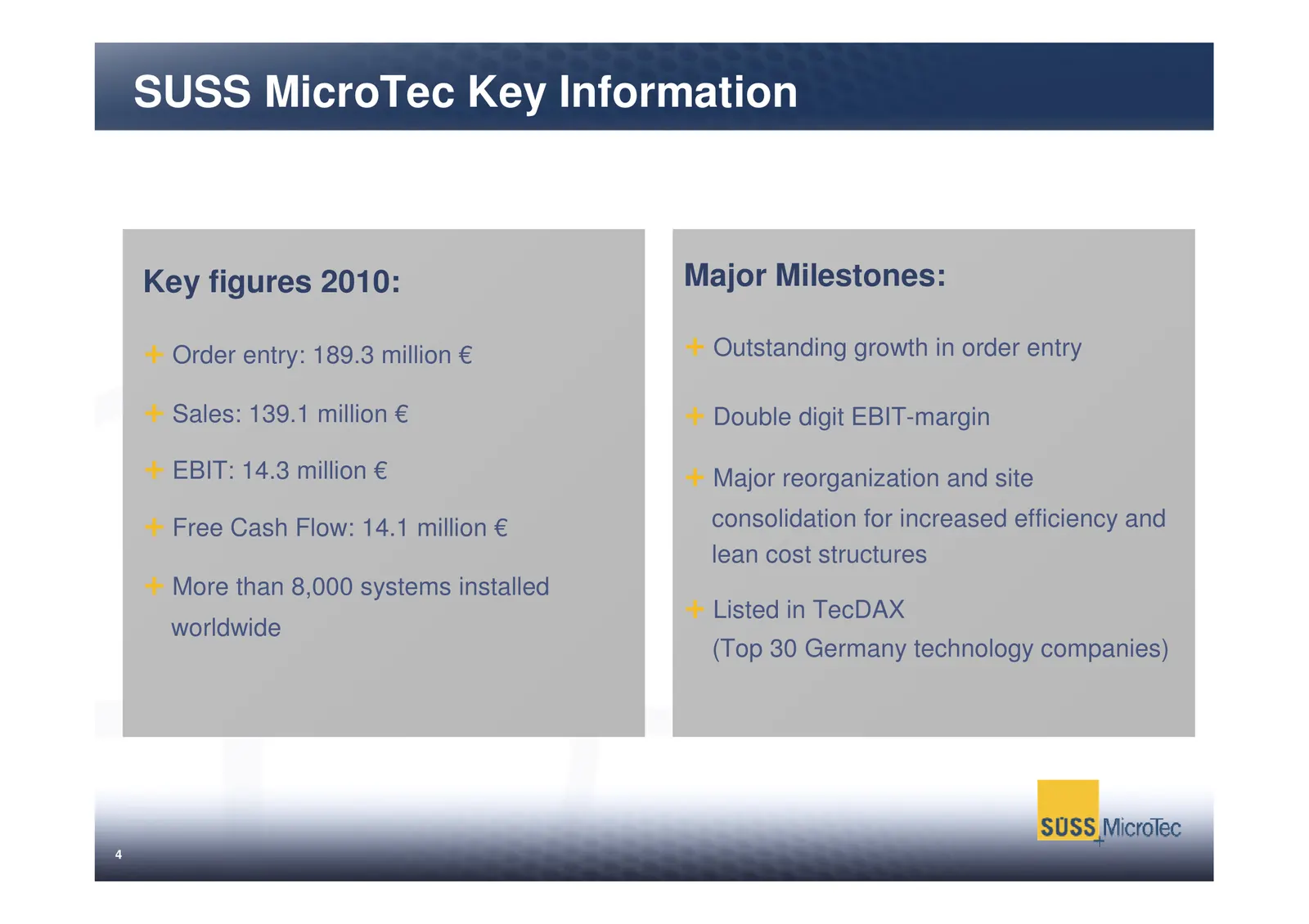
SUSS MicroTec Key Information Key figures 2010: Major Milestones: Order entry: 189.3 million € Outstanding growth in order entry Sales: 139.1 million € Double digit EBIT-margin EBIT: 14.3 million € Major reorganization and site Free Cash Flow: 14.1 million € consolidation for increased efficiency an
Slide 6: 12 Months Business Development
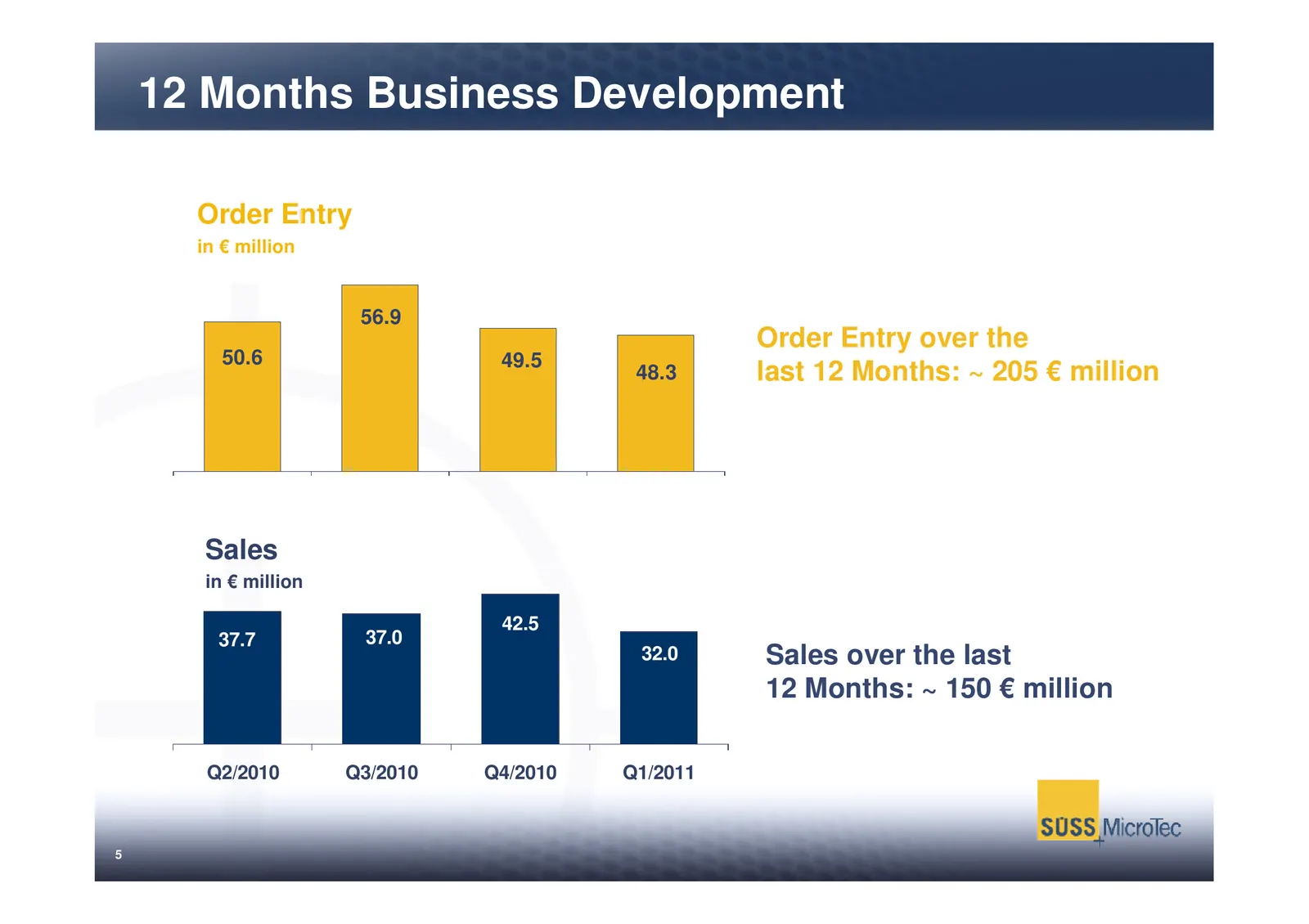
12 Months Business Development Order Entry in € million 56.9 Order Entry over the 50.6 49.5 48.3 last 12 Months: ~ 205 € million Sales in € million 42.5 37.7 37.0 32.0 Sales over the last 12 Months: ~ 150 € million Q2/2010 Q3/2010 Q4/2010 Q1/2011 5
Slide 7: Stock Performance 2011
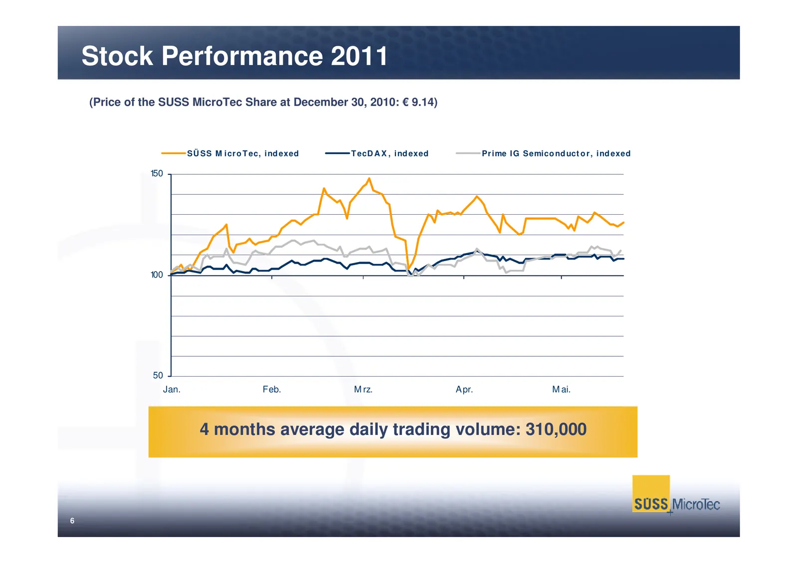
Stock Performance 2011 (Price of the SUSS MicroTec Share at December 30, 2010: € 9.14) SÜ SS M i cr o T ec, i nd exed T ecD A X , i nd exed Pr i me I G Semico nd uct o r , i nd exed 150 100 50 Jan. Feb. M rz. A pr. M ai. 4 months average daily trading volume: 310,000 6
Slide 8: Content
Content I. Executive Summary II. Products and Markets III. Growth Opportunities IV. Financials V. Outlook VI. Appendix 7
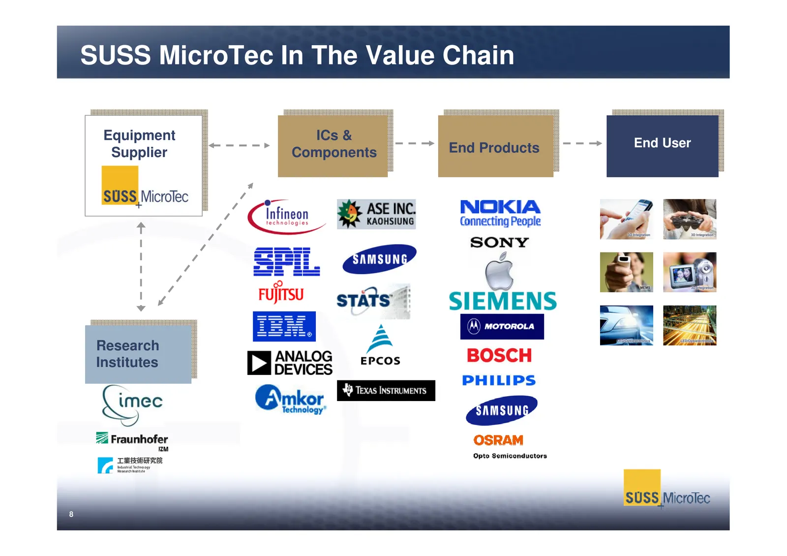
Slide 9: SUSS MicroTec In The Value Chain
SUSS MicroTec In The Value Chain Equipment ICs & End Products End User Supplier Components Research Institutes 8
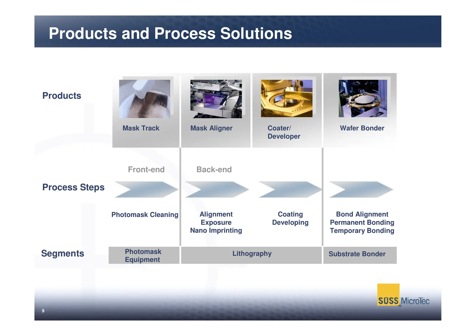
Slide 10: Products and Process Solutions
Products and Process Solutions Products Mask Track Mask Aligner Coater/ Wafer Bonder Developer Front-end Back-end Process Steps Photomask Cleaning Alignment Coating Bond Alignment Exposure Developing Permanent Bonding Nano Imprinting Temporary Bonding Segments Photomask Lithography Substrate Bonder
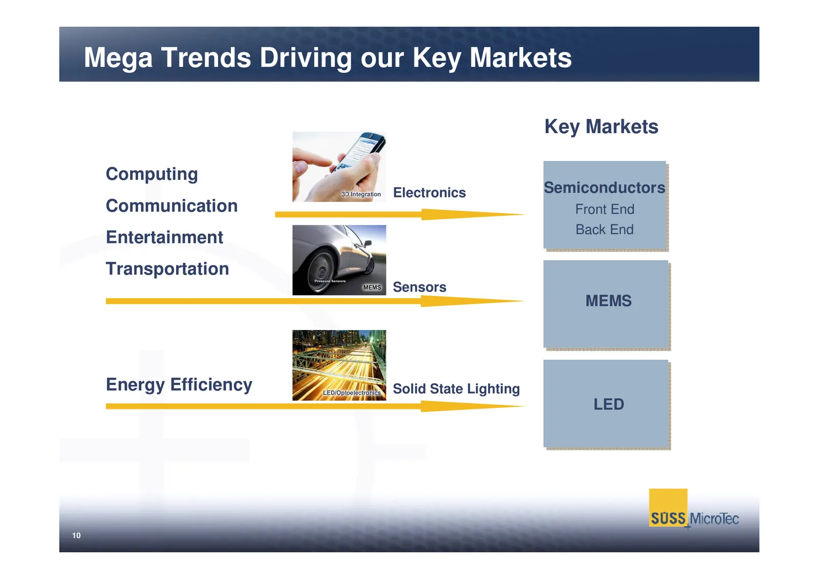
Slide 11: Mega Trends Driving our Key Markets
Mega Trends Driving our Key Markets Key Markets Computing Electronics Semiconductors Communication Front End Back End Entertainment Transportation Sensors MEMS Energy Efficiency Solid State Lighting LED 10
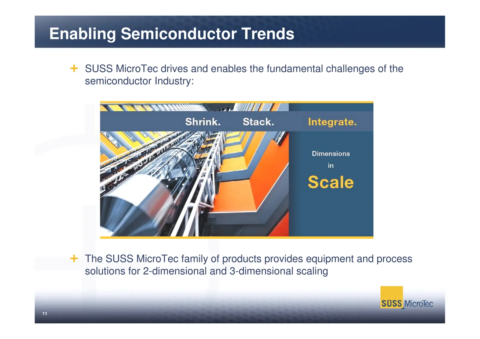
Slide 12: Enabling Semiconductor Trends
Enabling Semiconductor Trends SUSS MicroTec drives and enables the fundamental challenges of the semiconductor Industry: The SUSS MicroTec family of products provides equipment and process solutions for 2-dimensional and 3-dimensional scaling 11
Slide 13: Semiconductors
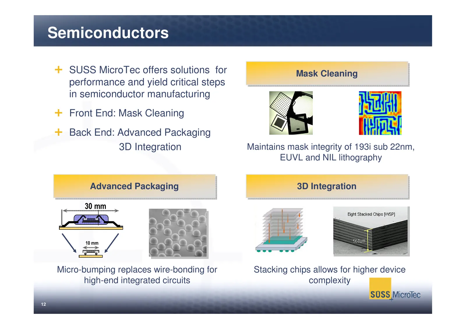
Semiconductors SUSS MicroTec offers solutions for Mask Mask Cleaning Cleaning performance and yield critical steps in semiconductor manufacturing Front End: Mask Cleaning Back End: Advanced Packaging 3D Integration Maintains mask integrity of 193i sub 22nm, EUVL and NIL lithography Advanced Advanced
Slide 14: MEMS and LED
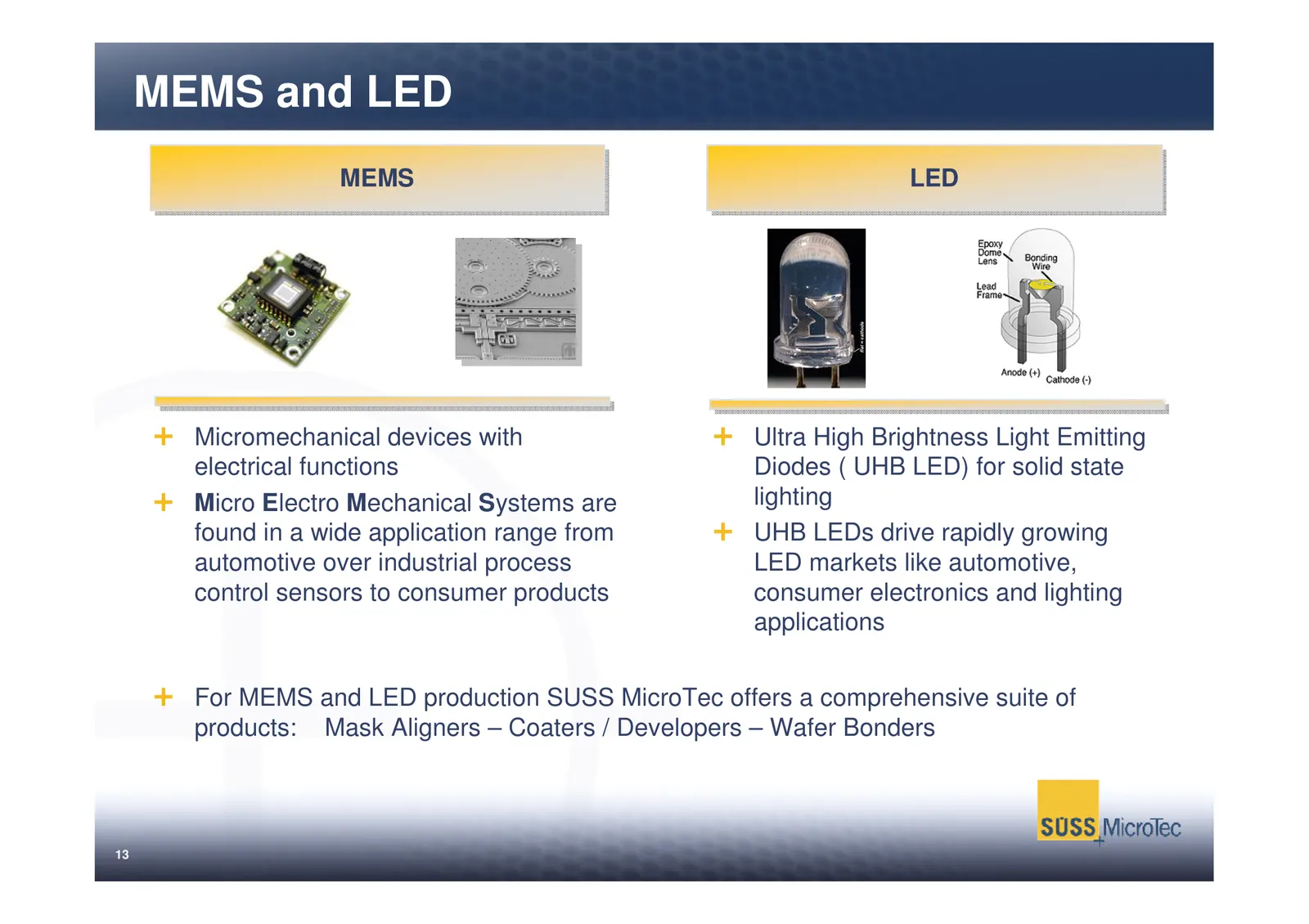
MEMS and LED MEMS MEMS LED LED Micromechanical devices with Ultra High Brightness Light Emitting electrical functions Diodes ( UHB LED) for solid state Micro Electro Mechanical Systems are lighting found in a wide application range from UHB LEDs drive rapidly growing automotive over industrial proce
Slide 15: From Advanced Packaging to 3D Integration
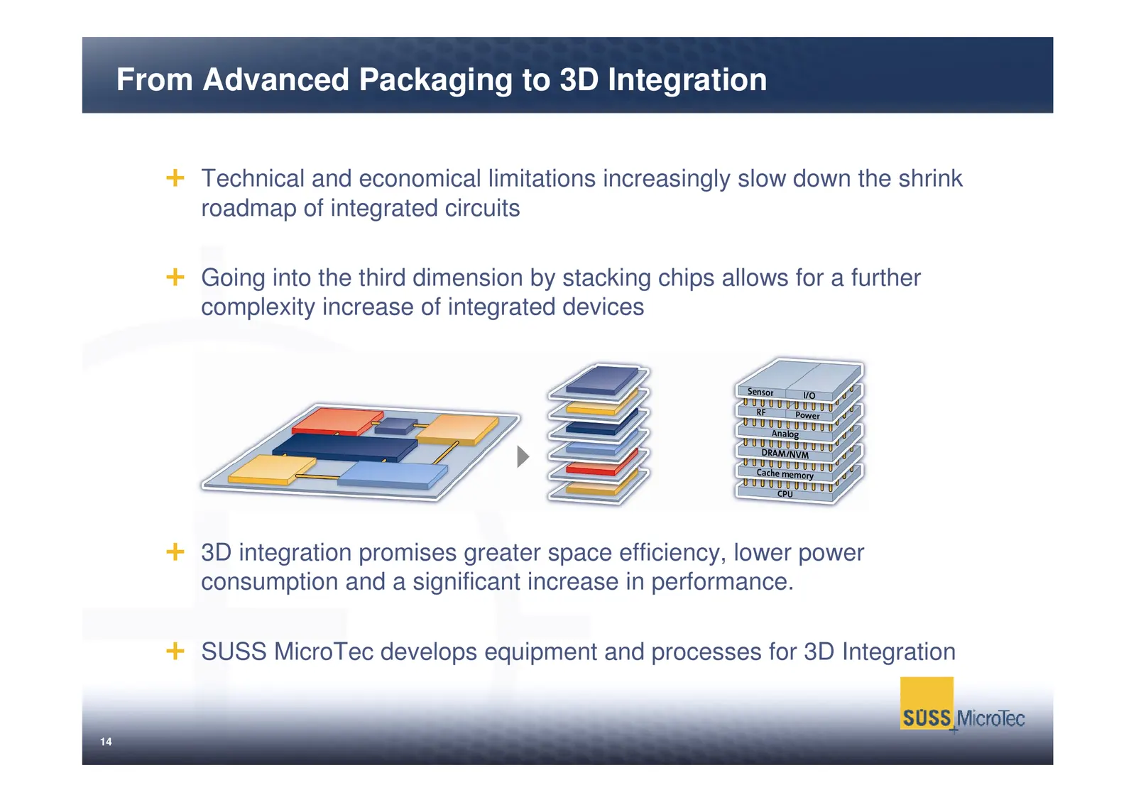
From Advanced Packaging to 3D Integration Technical and economical limitations increasingly slow down the shrink roadmap of integrated circuits Going into the third dimension by stacking chips allows for a further complexity increase of integrated devices 3D integration promises greater space effici
Slide 16: 3D Integration: Chip Design Using the Third Dimension
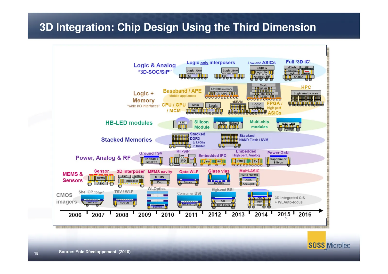
3D Integration: Chip Design Using the Third Dimension 15 Source: Yole Développement (2010)
Slide 17: Content
Content I. Executive Summary II. Products and Markets III. Growth Opportunities IV. Financials V. Outlook VI. Appendix 16
Slide 18: Growth Opportunities
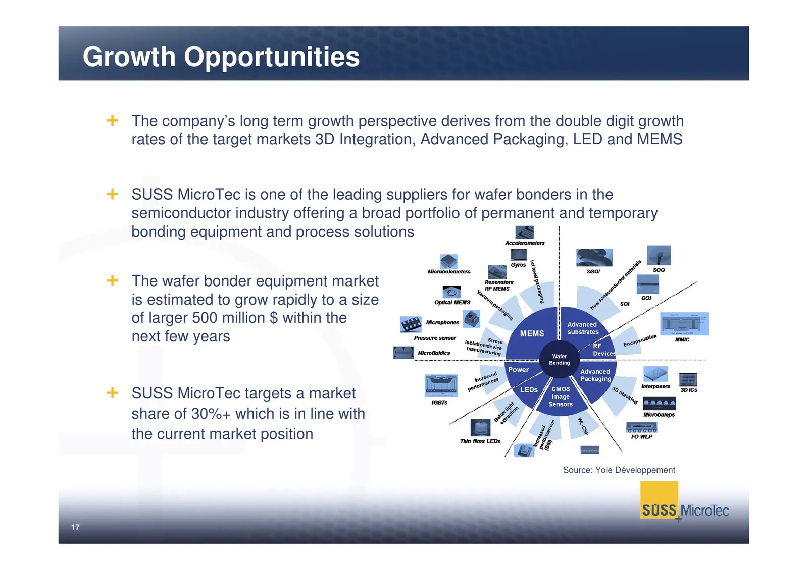
Growth Opportunities The company’s long term growth perspective derives from the double digit growth rates of the target markets 3D Integration, Advanced Packaging, LED and MEMS SUSS MicroTec is one of the leading suppliers for wafer bonders in the semiconductor industry offering a broad portfolio o
Slide 19: Enabling Growth: Production in Sternenfels
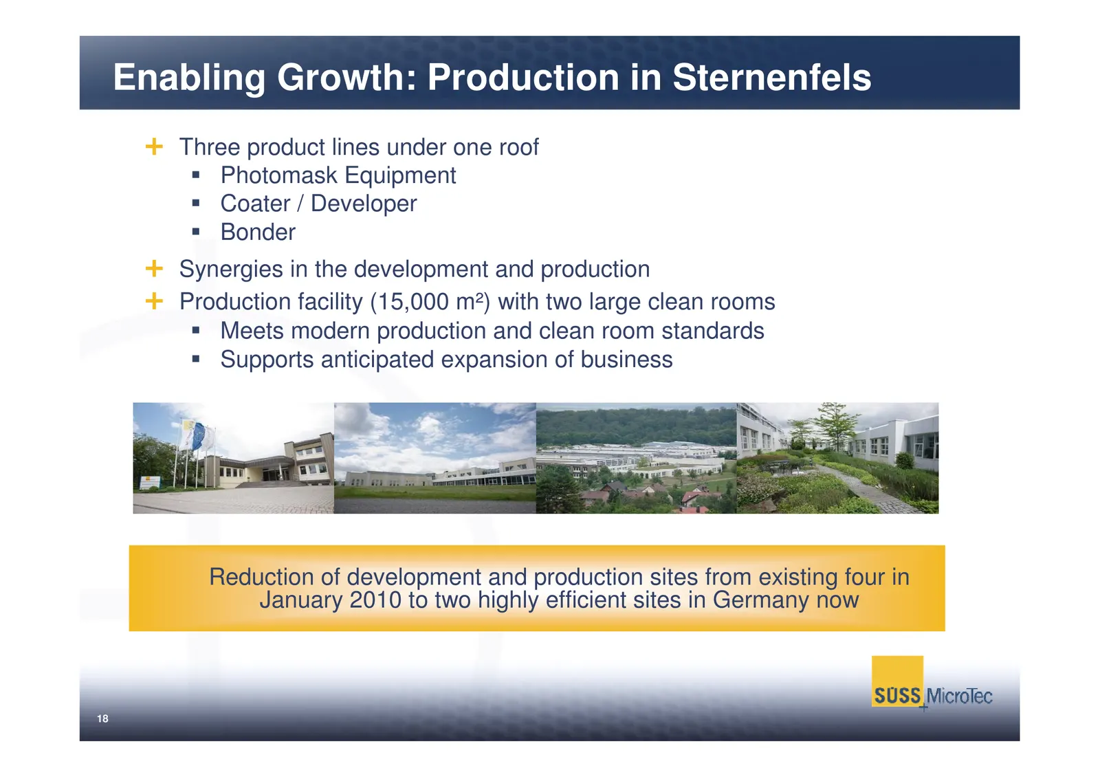
Enabling Growth: Production in Sternenfels Three product lines under one roof Photomask Equipment Coater / Developer Bonder Synergies in the development and production Production facility (15,000 m²) with two large clean rooms Meets modern production and clean room standards Supports anticipated exp
Slide 20: Enabling Growth: Differentiation
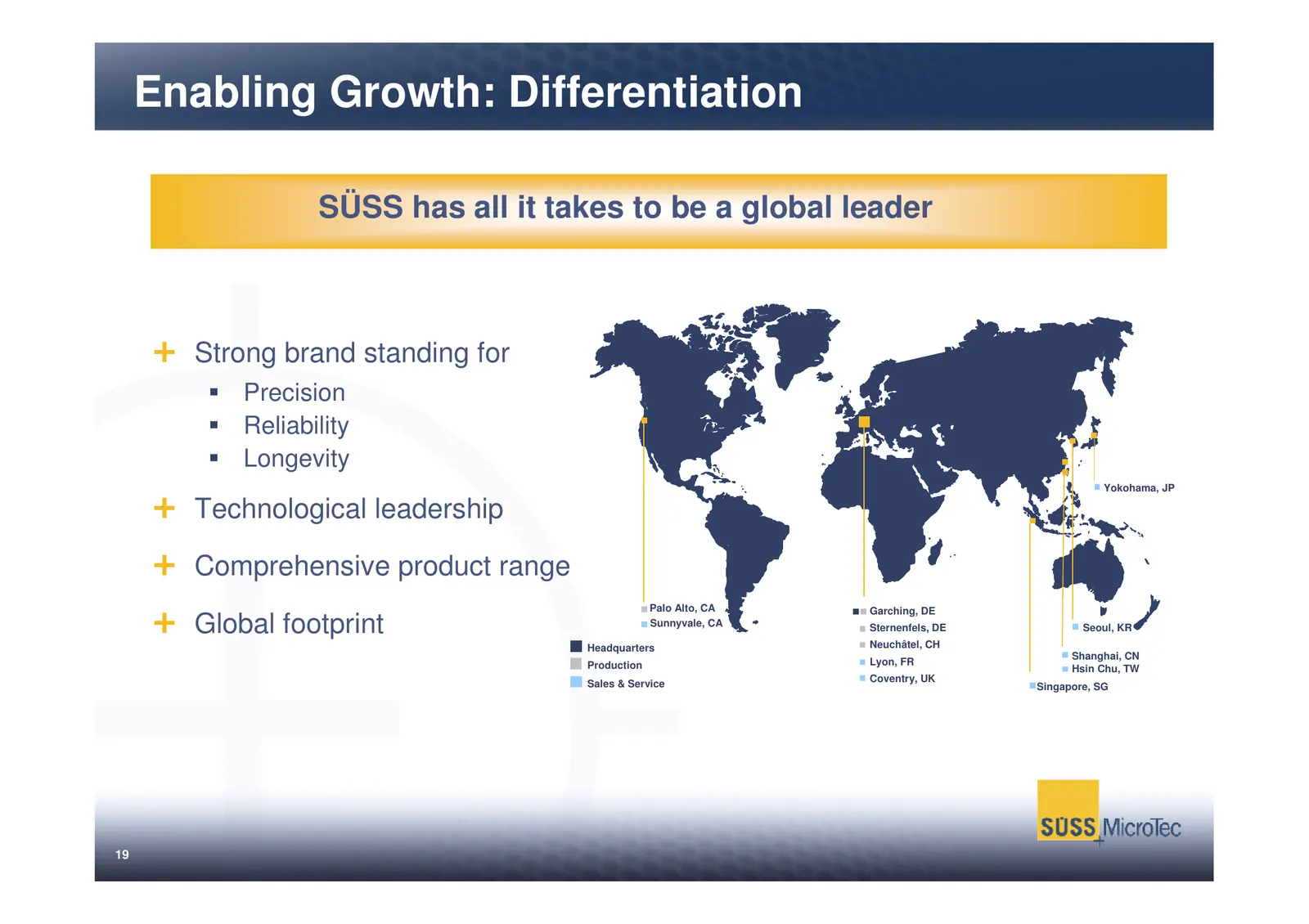
Enabling Growth: Differentiation SÜSS has all it takes to be a global leader Strong brand standing for Precision Reliability Longevity Yokohama, JP Technological leadership Comprehensive product range Palo Alto, CA Garching, DE Global footprint Sunnyvale, CA Sternenfels, DE Seoul, KR Headquarters Ne
Slide 21: Content
Content I. Executive Summary II. Products and Markets III. Growth Opportunities IV. Financials V. Outlook VI. Appendix 20
Slide 22: Key Financials
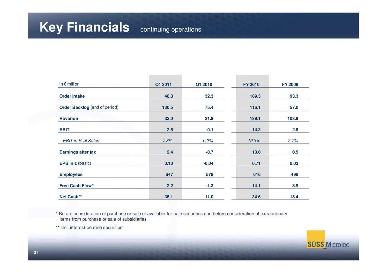
Key Financials continuing operations in € million Q1 2011 Q1 2010 FY 2010 FY 2009 Order Intake 48.3 32.3 189.3 93.3 Order Backlog (end of period) 130.5 75.4 116.1 57.0 Revenue 32.0 21.9 139.1 103.9 EBIT 2.5 -0.1 14.3 2.8 EBIT in % of Sales 7.8% -0.2% 10.3% 2.7% Earnings after tax 2.4 -0.7 13.0 0.5 E
Slide 23: Content
Content I. Executive Summary II. Products and Markets III. Growth Opportunities IV. Financials V. Outlook VI. Appendix 22
Slide 24: Outlook
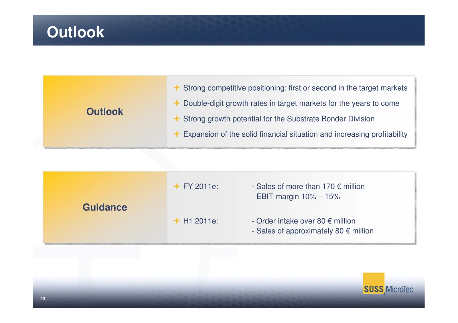
Outlook Strong competitive positioning: first or second in the target markets Double-digit growth rates in target markets for the years to come Outlook Outlook Strong growth potential for the Substrate Bonder Division Expansion of the solid financial situation and increasing profitability FY 2011e:
Slide 25: Investment case
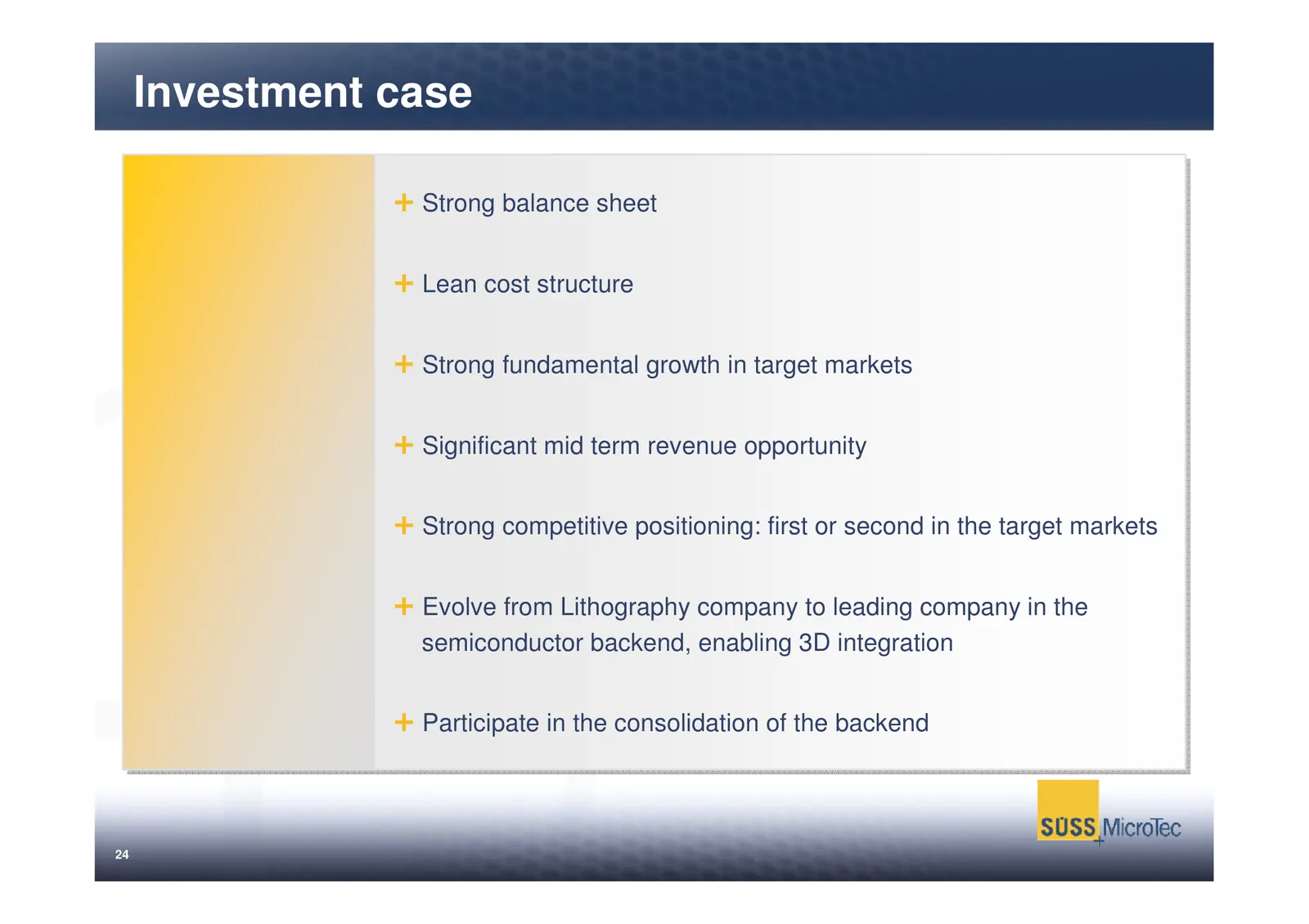
Investment case Strong balance sheet Lean cost structure Strong fundamental growth in target markets Significant mid term revenue opportunity Strong competitive positioning: first or second in the target markets Evolve from Lithography company to leading company in the semiconductor backend, enablin
Slide 26: Content
Content I. Executive Summary II. Products and Markets III. Growth Opportunities IV. Financials V. Outlook VI. Appendix 25
Slide 27: Long Term Development of the SUSS Share
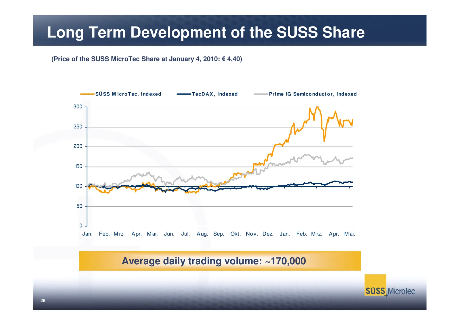
Long Term Development of the SUSS Share (Price of the SUSS MicroTec Share at January 4, 2010: € 4,40) SÜ SS M icr o T ec, ind exed T ecD A X , ind exed Pr ime IG Semico nd uct o r , ind exed 300 250 200 150 100 50 0 Jan. Feb. M rz. A pr. M ai. Jun. Jul. A ug. Sep. Okt. No v. Dez. Jan. Feb. M rz. A p
Slide 28: Ownership Information
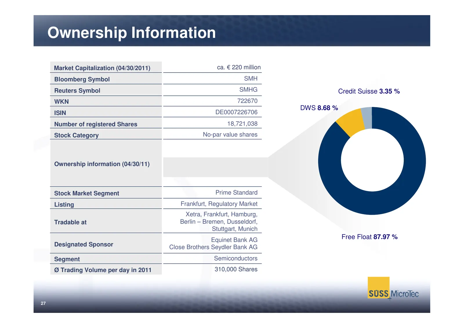
Ownership Information Market Capitalization (04/30/2011) ca. € 220 million Bloomberg Symbol SMH Reuters Symbol SMHG Credit Suisse 3.35 % WKN 722670 DWS 8.68 % ISIN DE0007226706 Number of registered Shares 18,721,038 Stock Category No-par value shares Ownership information (04/30/11) Stock Market Seg
Slide 29: Investor Relations Information
Investor Relations Information Contact Financial Calendar 2011 Franka Schielke Photonics Conference, Munich May 24 DZ Bank Sustainable Technologies Conference, Zurich June 8 Tel.: +49 (0) 89-32007- 161 Fax.: +49 (0) 89-32007- 451 UniCredit European Forum, San Francisco June 8 / 9 Email: franka.schie
Slide 30: Segment Reporting 2010
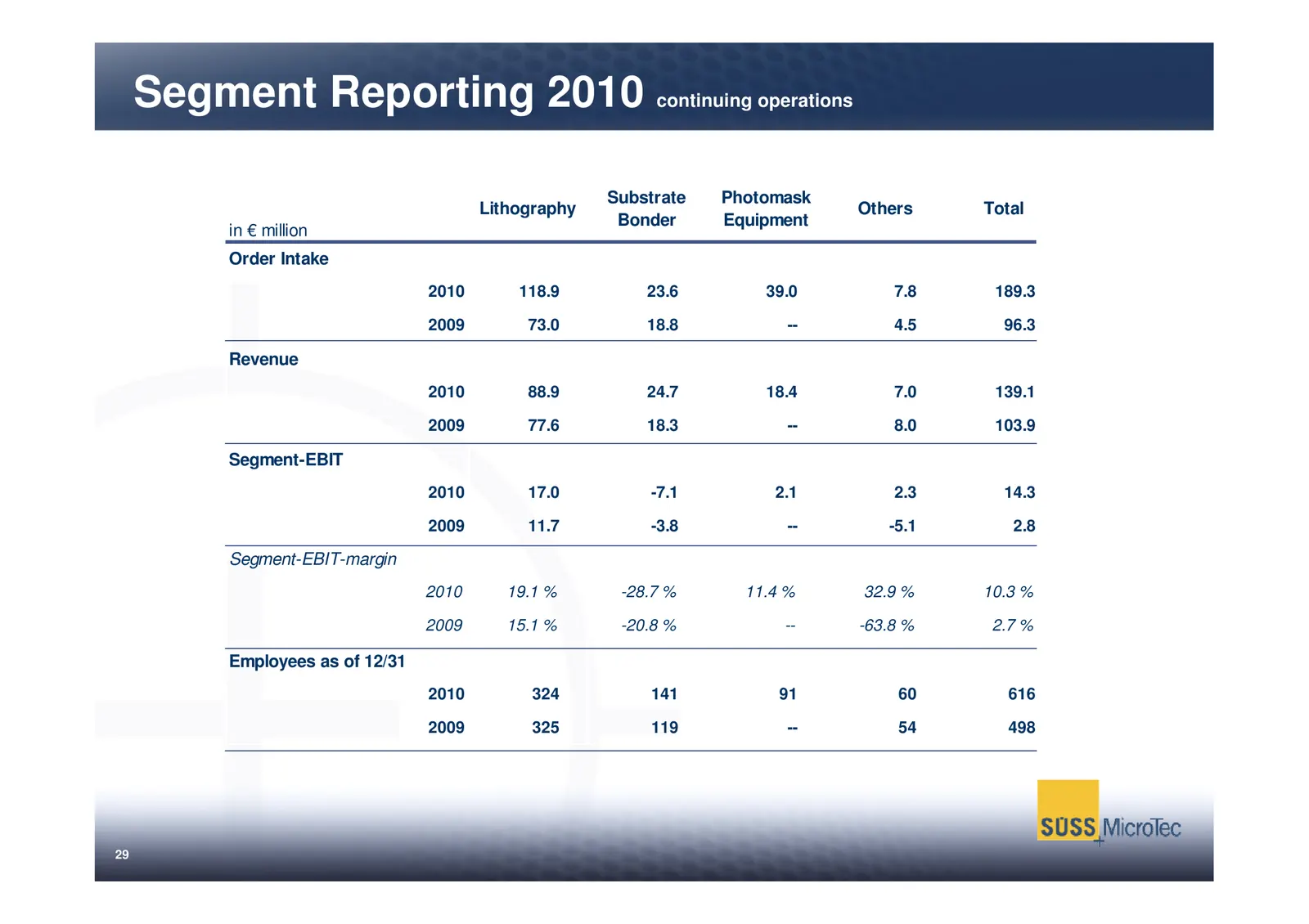
Segment Reporting 2010 continuing operations Substrate Photomask Lithography Others Total Bonder Equipment in € million Order Intake 2010 118.9 23.6 39.0 7.8 189.3 2009 73.0 18.8 -- 4.5 96.3 Revenue 2010 88.9 24.7 18.4 7.0 139.1 2009 77.6 18.3 -- 8.0 103.9 Segment-EBIT 2010 17.0 -7.1 2.1 2.3 14.3 20
Slide 31: Order Entry Analysis 2010
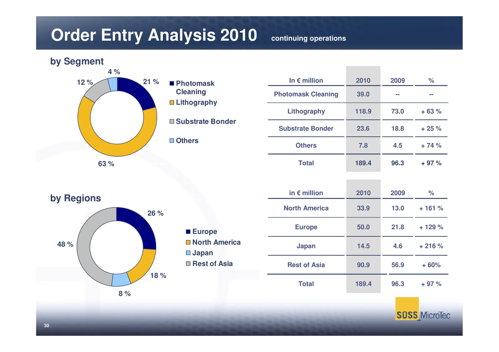
Order Entry Analysis 2010 continuing operations by Segment 4% 12 % 21 % Photomask In € million 2010 2009 % Cleaning Photomask Cleaning 39.0 -- -- Lithography Lithography 118.9 73.0 + 63 % Substrate Bonder Substrate Bonder 23.6 18.8 + 25 % Others Others 7.8 4.5 + 74 % 63 % Total 189.4 96.3 + 97 % in
Slide 32: Sales Analysis 2010
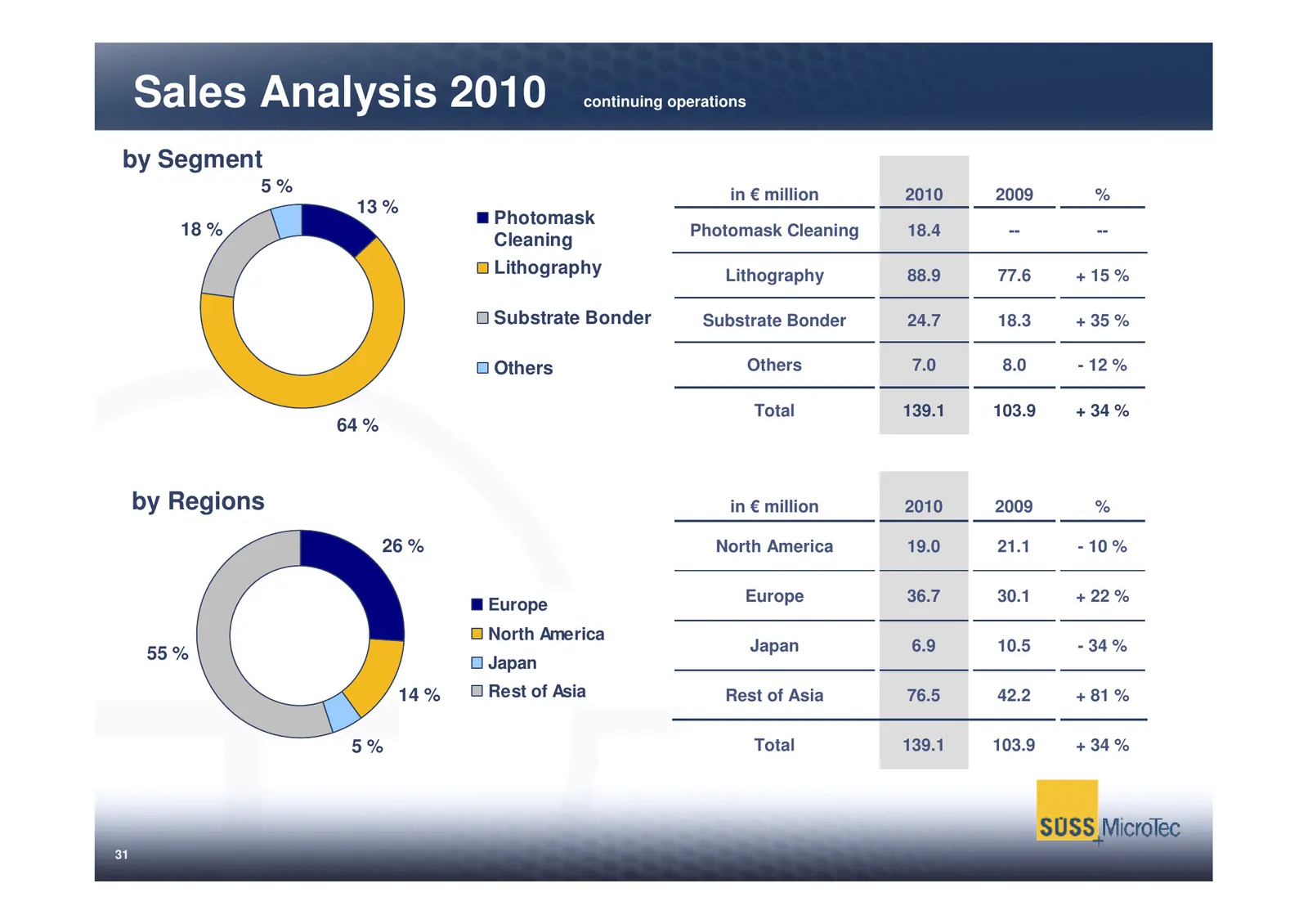
Sales Analysis 2010 continuing operations by Segment 5% in € million 2010 2009 % 13 % Photomask 18 % Photomask Cleaning 18.4 -- -- Cleaning Lithography Lithography 88.9 77.6 + 15 % Substrate Bonder Substrate Bonder 24.7 18.3 + 35 % Others Others 7.0 8.0 - 12 % Total 139.1 103.9 + 34 % 64 % by Region
Slide 33: SUSS Management Board
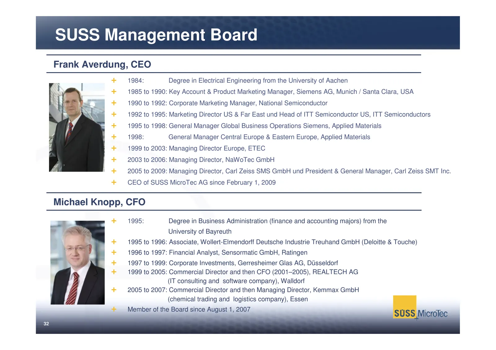
SUSS Management Board Frank Averdung, CEO 1984: Degree in Electrical Engineering from the University of Aachen 1985 to 1990: Key Account & Product Marketing Manager, Siemens AG, Munich / Santa Clara, USA 1990 to 1992: Corporate Marketing Manager, National Semiconductor 1992 to 1995: Marketing Direct
Slide 34: Strategic Restructuring Measures
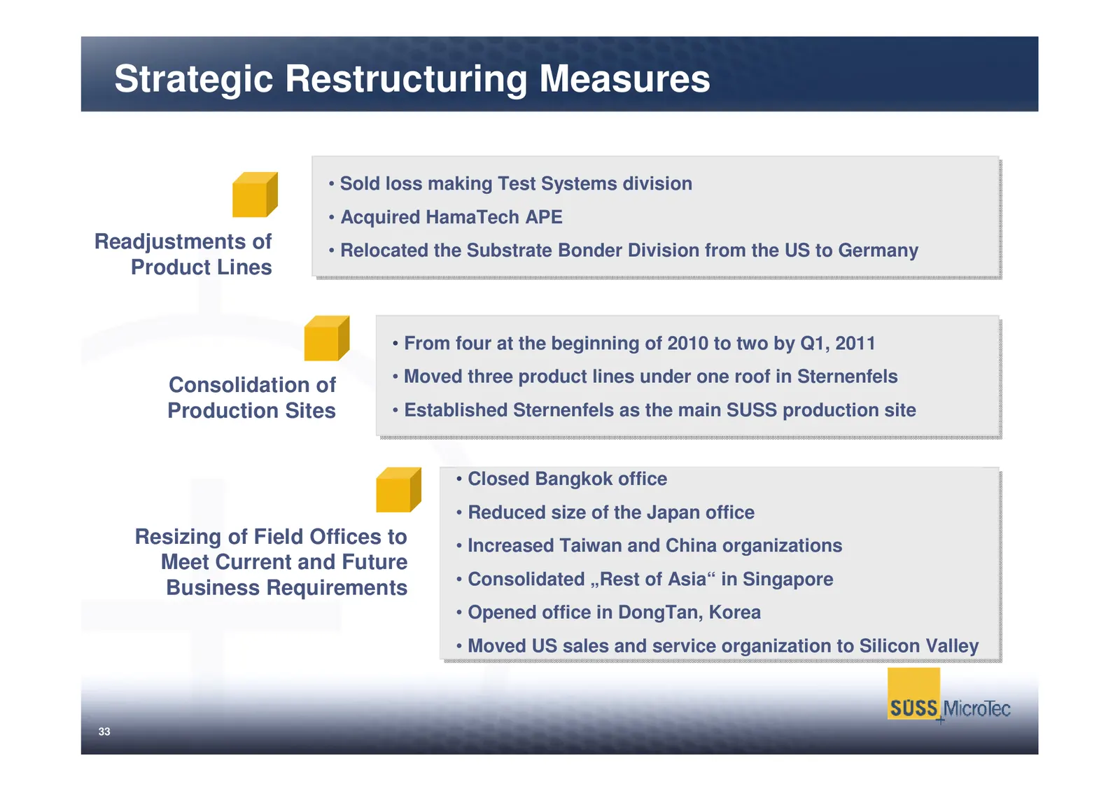
Strategic Restructuring Measures • Sold loss making Test Systems division • Acquired HamaTech APE Readjustments of • Relocated the Substrate Bonder Division from the US to Germany Product Lines • From four at the beginning of 2010 to two by Q1, 2011 Consolidation of • Moved three product lines under
Slide 35: Photomask / NIL Markets & Technologies
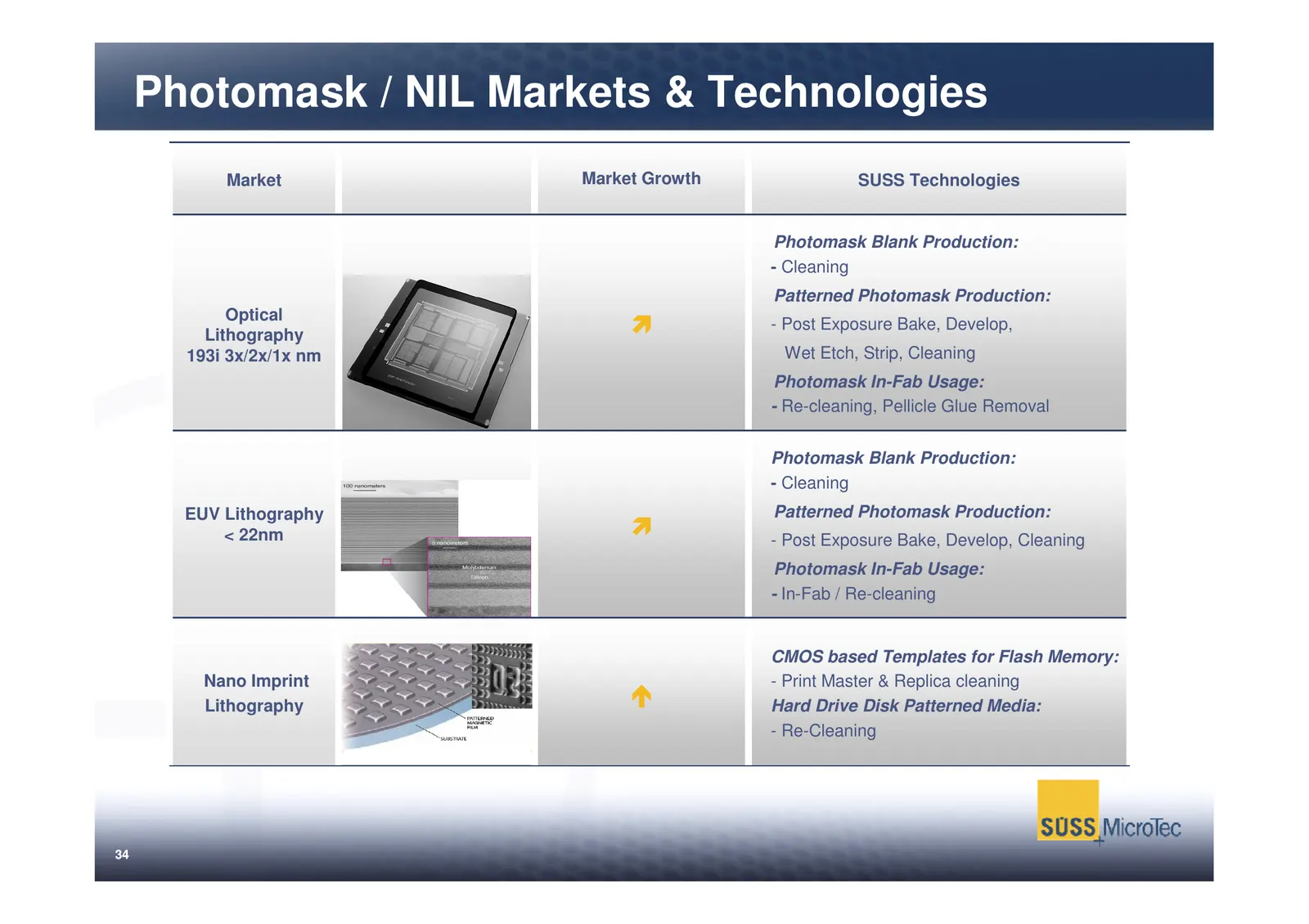
Photomask / NIL Markets & Technologies Market Market Growth SUSS Technologies Photomask Blank Production: - Cleaning Patterned Photomask Production: Optical Lithography - Post Exposure Bake, Develop, 193i 3x/2x/1x nm Wet Etch, Strip, Cleaning Photomask In-Fab Usage: - Re-cleaning, Pellicle Glue Remo
Slide 36: Aligner Markets & Technologies
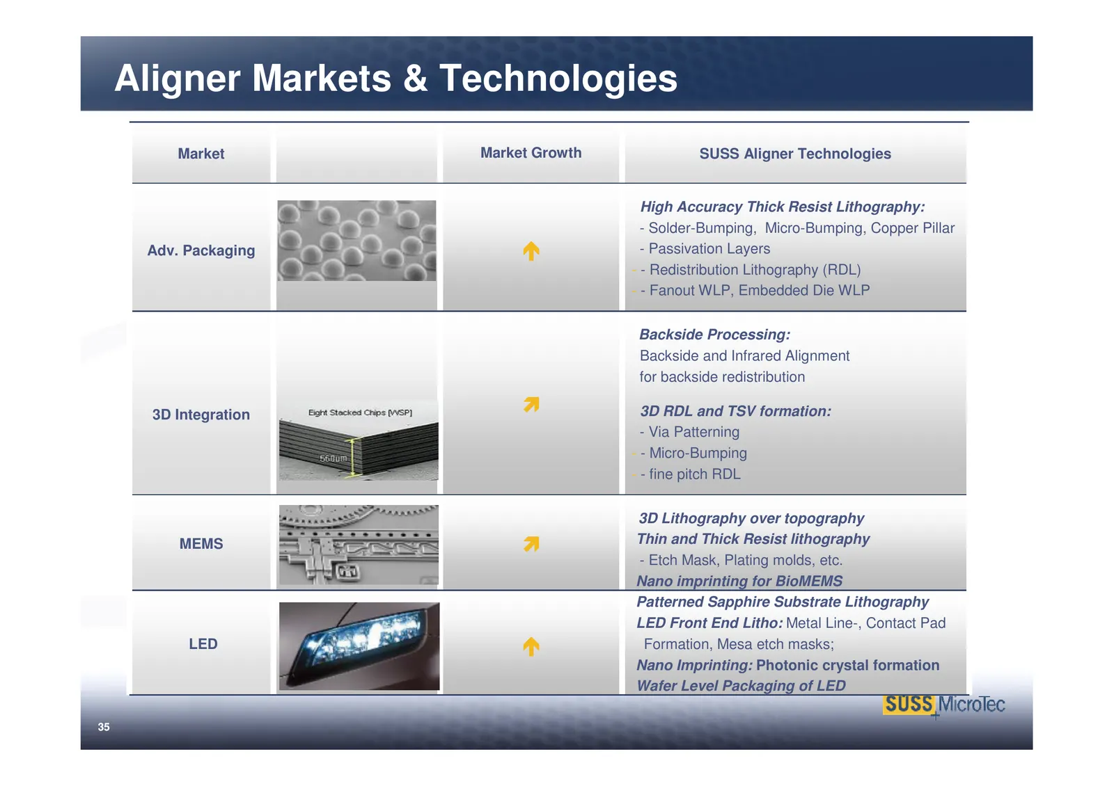
Aligner Markets & Technologies Market Market Growth SUSS Aligner Technologies High Accuracy Thick Resist Lithography: - Solder-Bumping, Micro-Bumping, Copper Pillar Adv. Packaging - Passivation Layers - - Redistribution Lithography (RDL) - - Fanout WLP, Embedded Die WLP Backside Processing: Backside
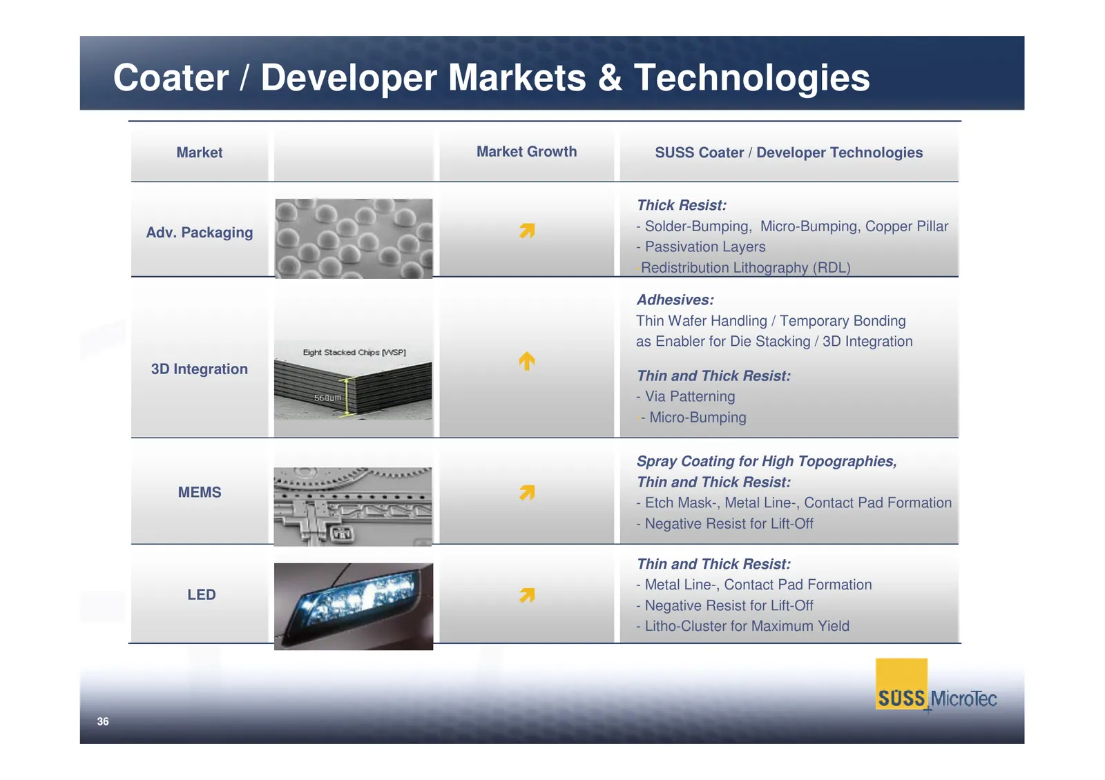
Slide 37: Coater / Developer Markets & Technologies
Coater / Developer Markets & Technologies Market Market Growth SUSS Coater / Developer Technologies Thick Resist: - Solder-Bumping, Micro-Bumping, Copper Pillar Adv. Packaging - Passivation Layers -Redistribution Lithography (RDL) Adhesives: Thin Wafer Handling / Temporary Bonding as Enabler for Die
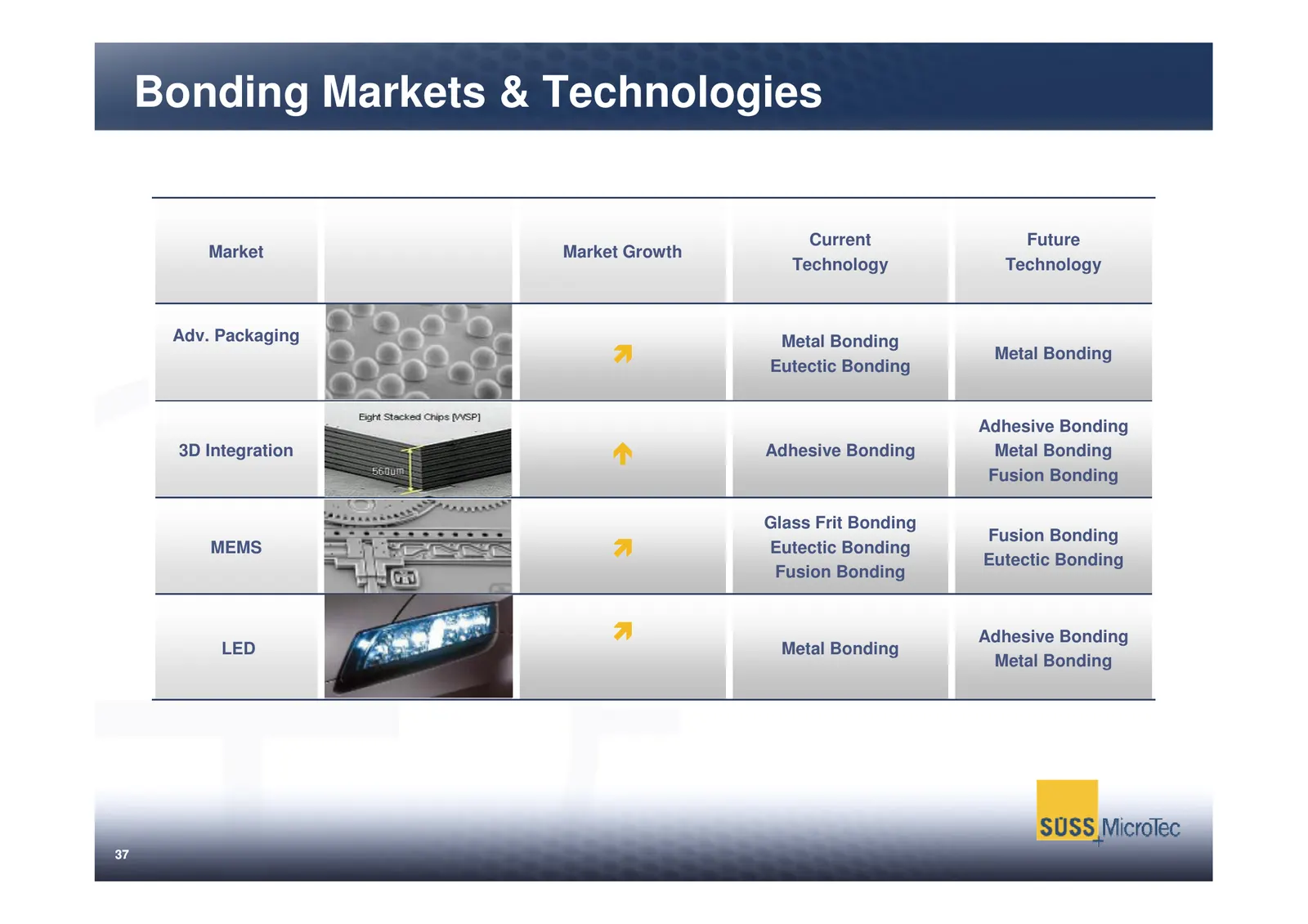
Slide 38: Bonding Markets & Technologies
Bonding Markets & Technologies Current Future Market Market Growth Technology Technology Adv. Packaging Metal Bonding Metal Bonding Eutectic Bonding Adhesive Bonding 3D Integration Adhesive Bonding Metal Bonding Fusion Bonding Glass Frit Bonding Fusion Bonding MEMS Eutectic Bonding Eutectic Bonding
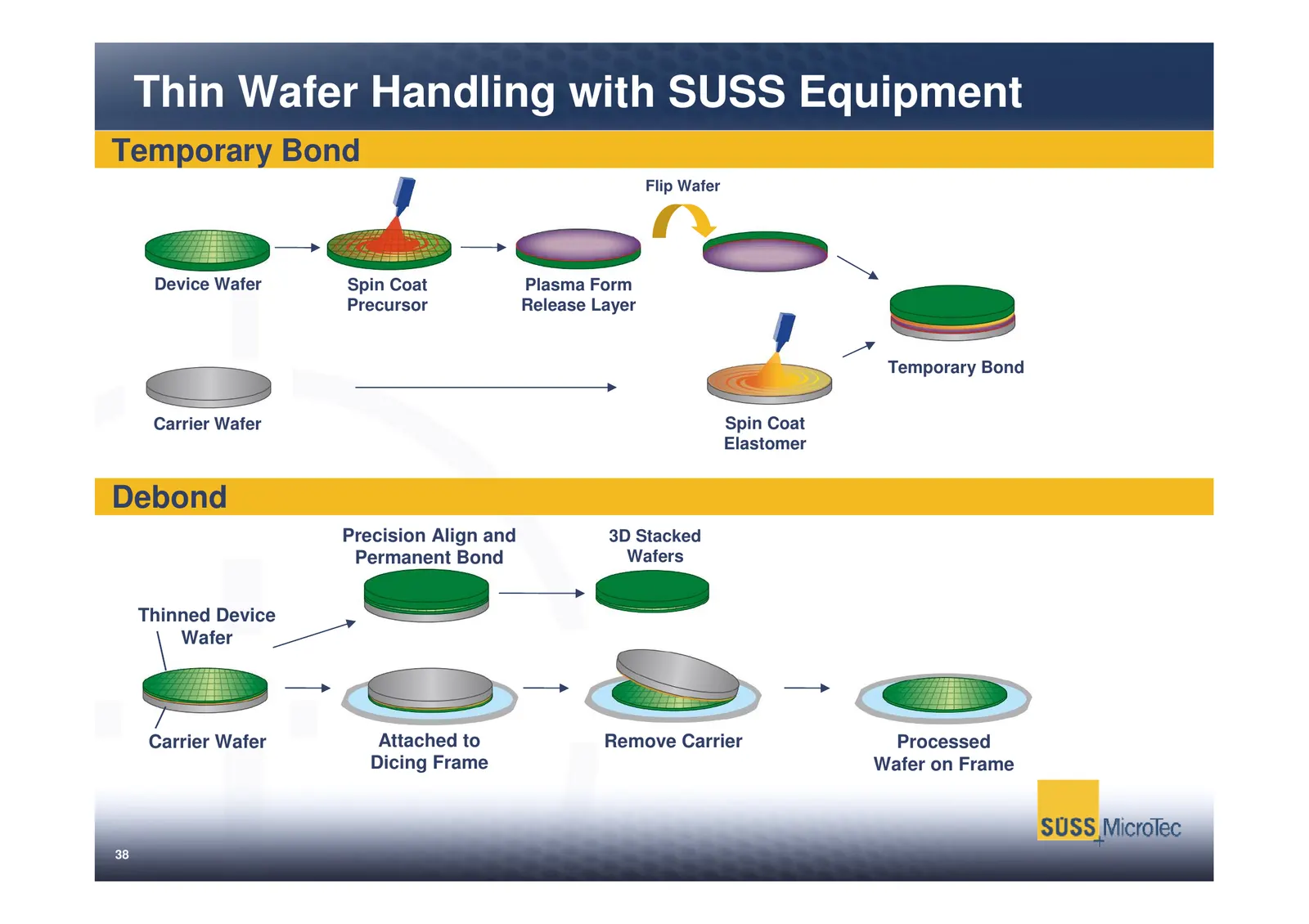
Slide 39: Thin Wafer Handling with SUSS Equipment
Thin Wafer Handling with SUSS Equipment Temporary Bond Flip Wafer Device Wafer Spin Coat Plasma Form Precursor Release Layer Temporary Bond Carrier Wafer Spin Coat Elastomer Debond Precision Align and 3D Stacked Permanent Bond Wafers Thinned Device Wafer Carrier Wafer Attached to Remove Carrier Proc
Source: Internet Archive copy of suss.com
More decks from SUSS MicroTec SE
 9M 2026 Earnings Presentation23 slides · Nov 5, 2026
 Investor Presentation (October 2026)41 slides · October 2026
 H1 2026 Earnings Presentation24 slides · Aug 6, 2026
 Q1 2026 Earnings Presentation19 slides · May 7, 2026
 FY2025 Earnings Presentation26 slides · Mar 30, 2026
 Investor Presentation (March 2026)42 slides · Mar 1, 2026