SUSS MicroTec SE · XETR:SMHN
SUSS MicroTec — Motorola — Technical Presentation (October 2003)
50 slides from SUSS MicroTec's technical presentation, Oct 9, 2003
Slide 1: Challenges in Packaging for MEMS devices
Challenges in Packaging for MEMS devices BISHNU GOGOI Ph.D. Distinguished Member of the Technical Staff Sensor Technology Development Motorola Sensor Products Division BISHNU GOGOI, SENSOR PRODUCTS DIVISION SLIDE 1, 9 OCTOBER 2003 MOTOROLA GENERAL BUSINESS
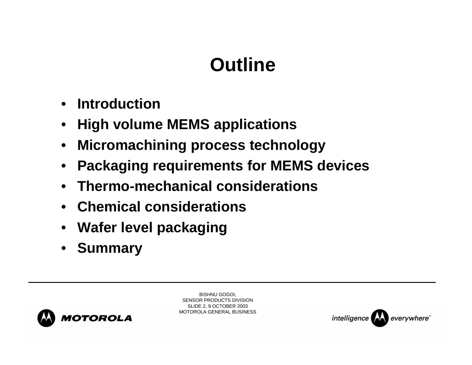
Slide 2: Outline
Outline • Introduction • High volume MEMS applications • Micromachining process technology • Packaging requirements for MEMS devices • Thermo-mechanical considerations • Chemical considerations • Wafer level packaging • Summary BISHNU GOGOI, SENSOR PRODUCTS DIVISION SLIDE 2, 9 OCTOBER 2003 MOTOROLA
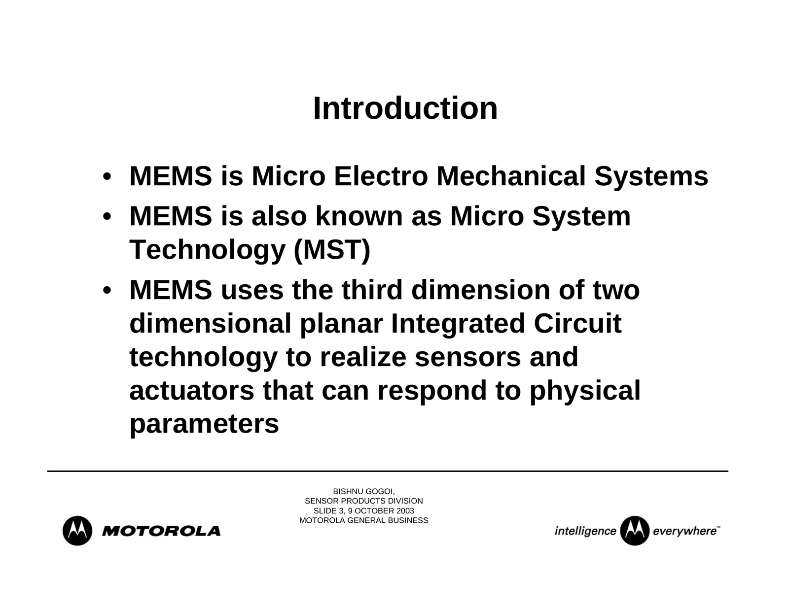
Slide 3: Introduction
Introduction • MEMS is Micro Electro Mechanical Systems • MEMS is also known as Micro System Technology (MST) • MEMS uses the third dimension of two dimensional planar Integrated Circuit technology to realize sensors and actuators that can respond to physical parameters BISHNU GOGOI, SENSOR PRODUCTS
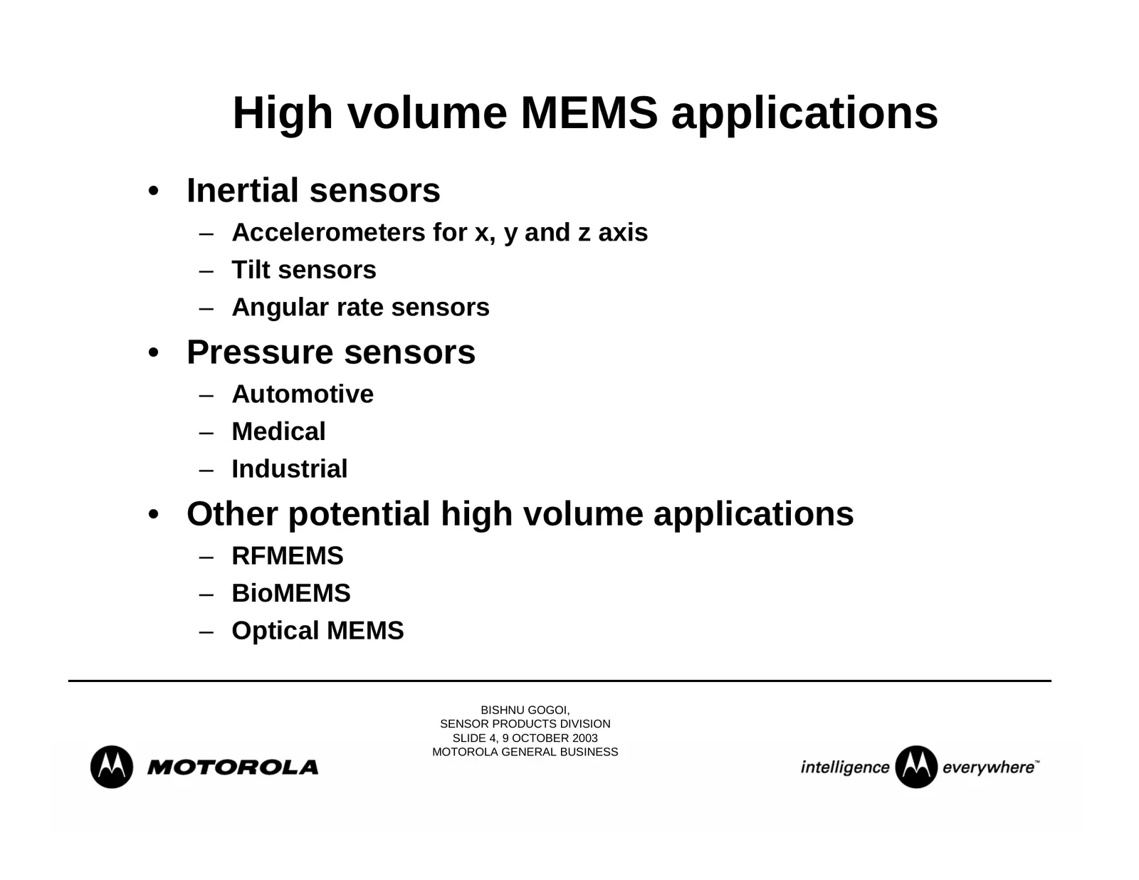
Slide 4: High volume MEMS applications
High volume MEMS applications • Inertial sensors – Accelerometers for x, y and z axis – Tilt sensors – Angular rate sensors • Pressure sensors – Automotive – Medical – Industrial • Other potential high volume applications – RFMEMS – BioMEMS – Optical MEMS BISHNU GOGOI, SENSOR PRODUCTS DIVISION SLIDE
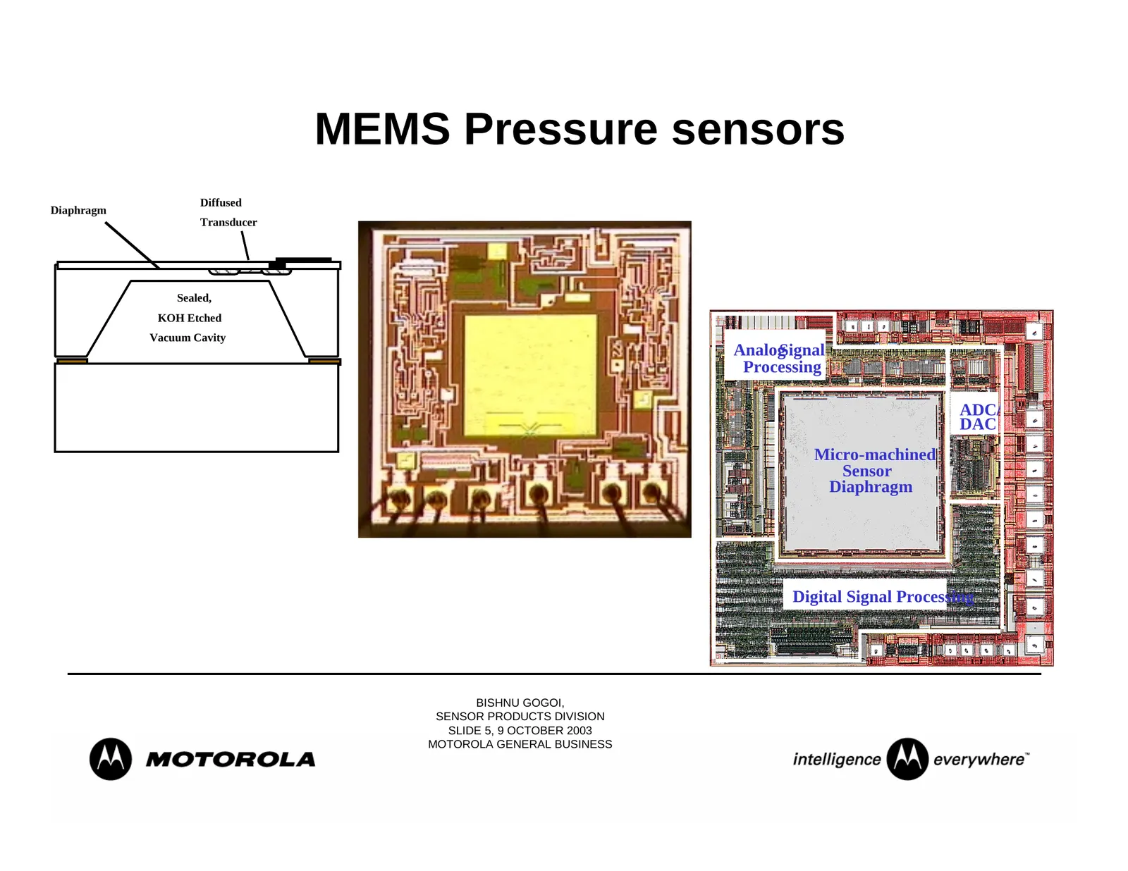
Slide 5: MEMS Pressure sensors
MEMS Pressure sensors Diffused Diaphragm Transducer Sealed, KOH Etched Vacuum Cavity AnalogSignal Processing ADC/ DAC Micro-machined Sensor Diaphragm Digital Signal Processing BISHNU GOGOI, SENSOR PRODUCTS DIVISION SLIDE 5, 9 OCTOBER 2003 MOTOROLA GENERAL BUSINESS
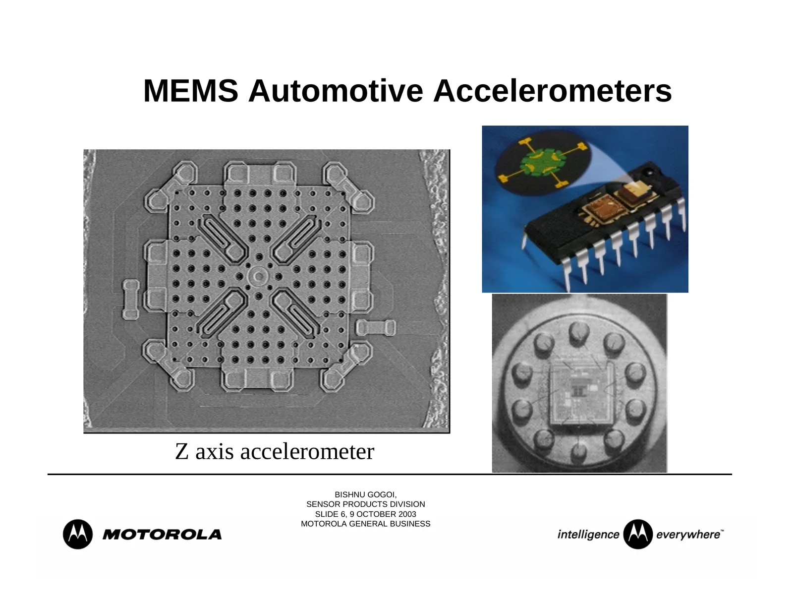
Slide 6: MEMS Automotive Accelerometers
MEMS Automotive Accelerometers Z axis accelerometer BISHNU GOGOI, SENSOR PRODUCTS DIVISION SLIDE 6, 9 OCTOBER 2003 MOTOROLA GENERAL BUSINESS
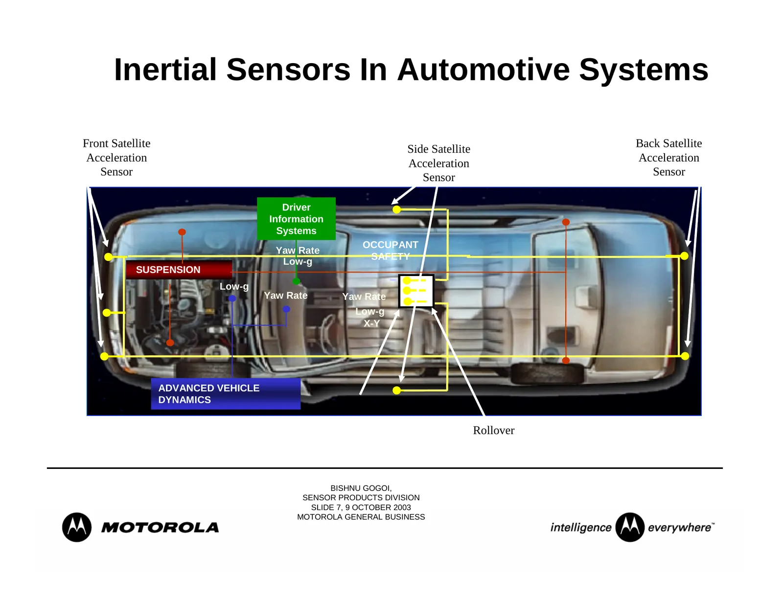
Slide 7: Inertial Sensors In Automotive Systems
Inertial Sensors In Automotive Systems Front Satellite Side Satellite Back Satellite Acceleration Acceleration Acceleration Sensor Sensor Sensor Driver Information Systems OCCUPANT Yaw Rate Low-g SAFETY SUSPENSION Low-g Yaw Rate Yaw Rate Low-g X-Y Central Crash ADVANCED VEHICLE Sensor DYNAMICS Rollo
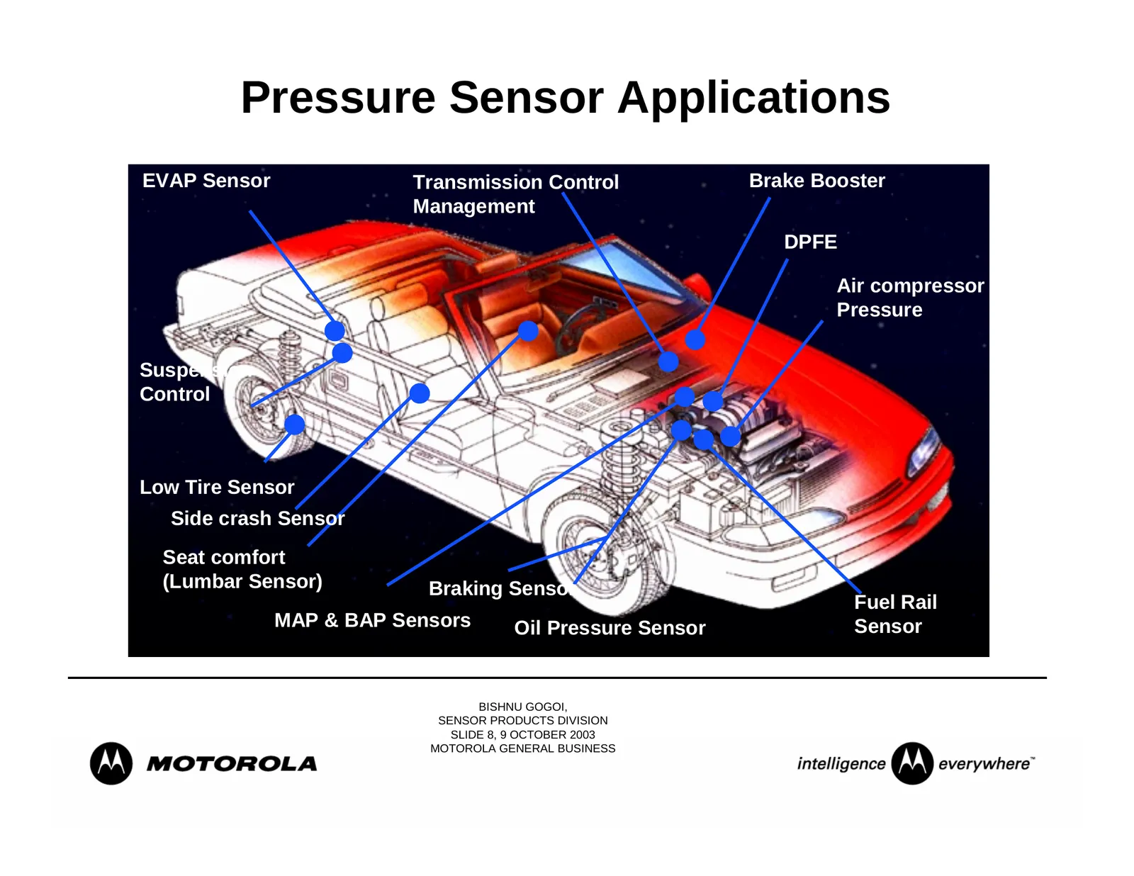
Slide 8: Pressure Sensor Applications
Pressure Sensor Applications EVAP Sensor Transmission Control Brake Booster Management DPFE Air compressor Pressure Suspension Control Low Tire Sensor Side crash Sensor Seat comfort (Lumbar Sensor) Braking Sensor Fuel Rail MAP & BAP Sensors Oil Pressure Sensor Sensor BISHNU GOGOI, SENSOR PRODUCTS DI
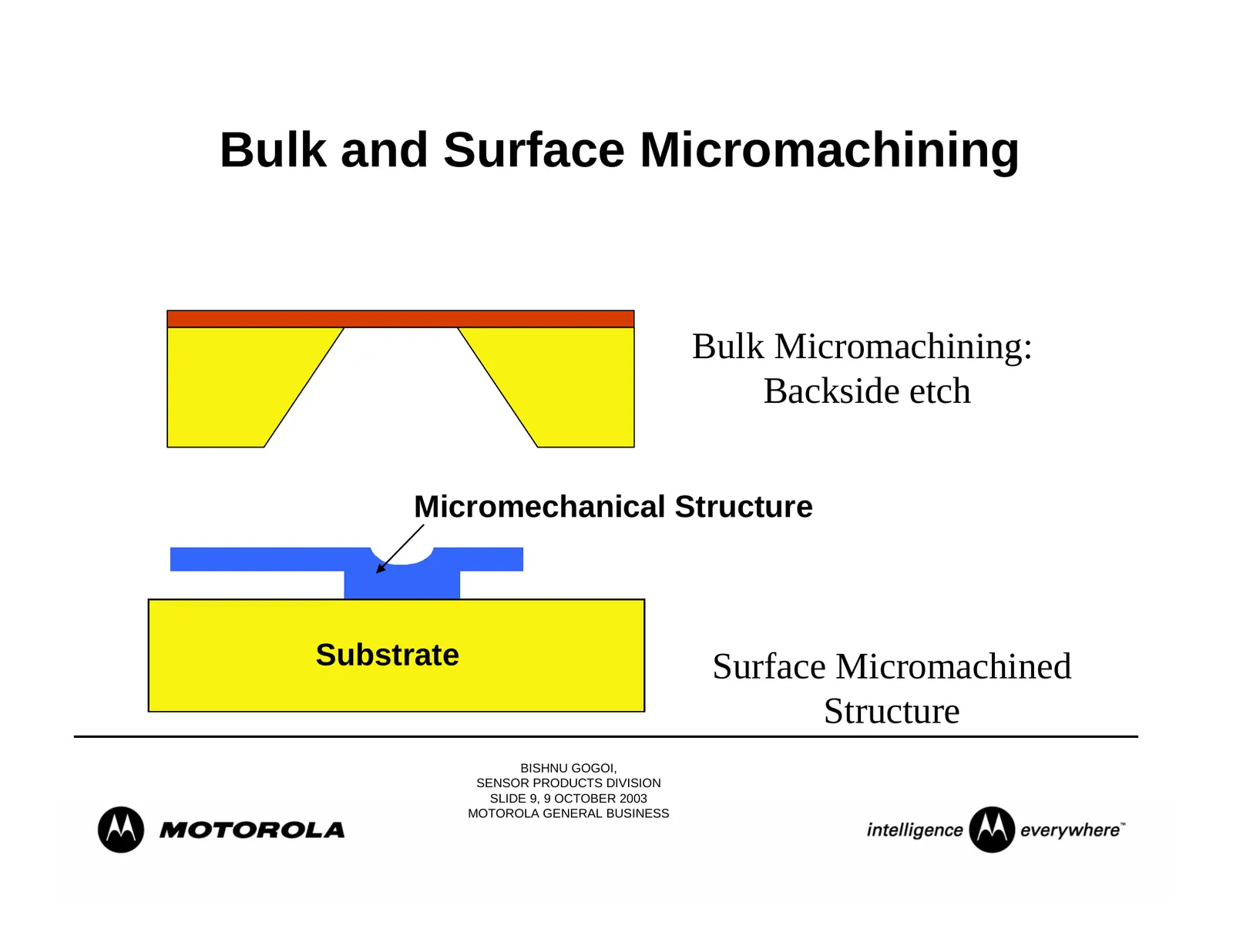
Slide 9: Bulk and Surface Micromachining
Bulk and Surface Micromachining Bulk Micromachining: Backside etch Micromechanical Structure Substrate Surface Micromachined Structure BISHNU GOGOI, SENSOR PRODUCTS DIVISION SLIDE 9, 9 OCTOBER 2003 MOTOROLA GENERAL BUSINESS
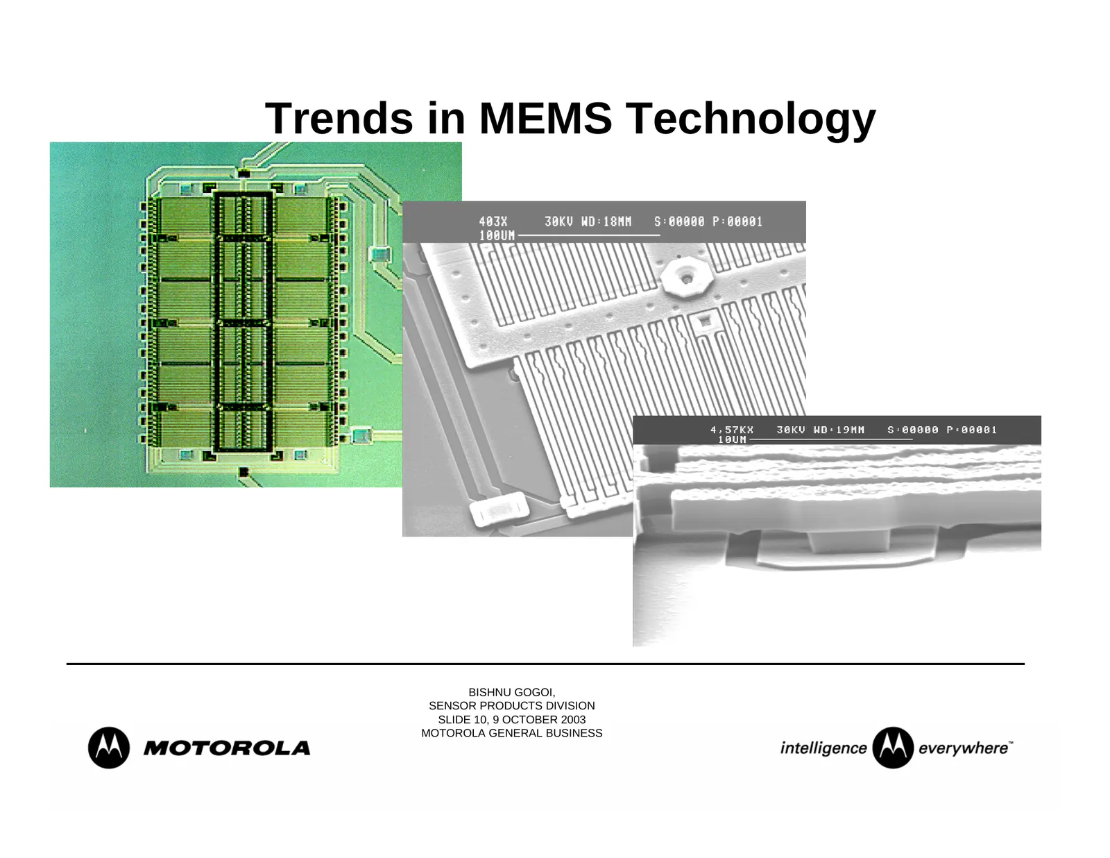
Slide 10: Trends in MEMS Technology
Trends in MEMS Technology BISHNU GOGOI, SENSOR PRODUCTS DIVISION SLIDE 10, 9 OCTOBER 2003 MOTOROLA GENERAL BUSINESS
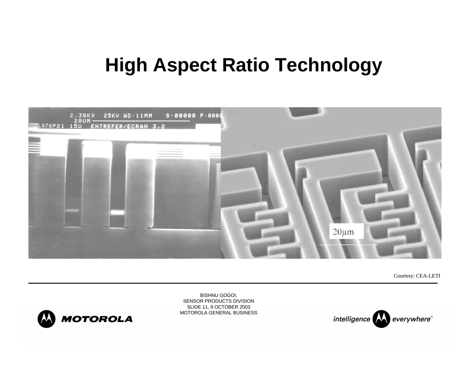
Slide 11: High Aspect Ratio Technology
High Aspect Ratio Technology Courtesy: CEA-LETI BISHNU GOGOI, SENSOR PRODUCTS DIVISION SLIDE 11, 9 OCTOBER 2003 MOTOROLA GENERAL BUSINESS
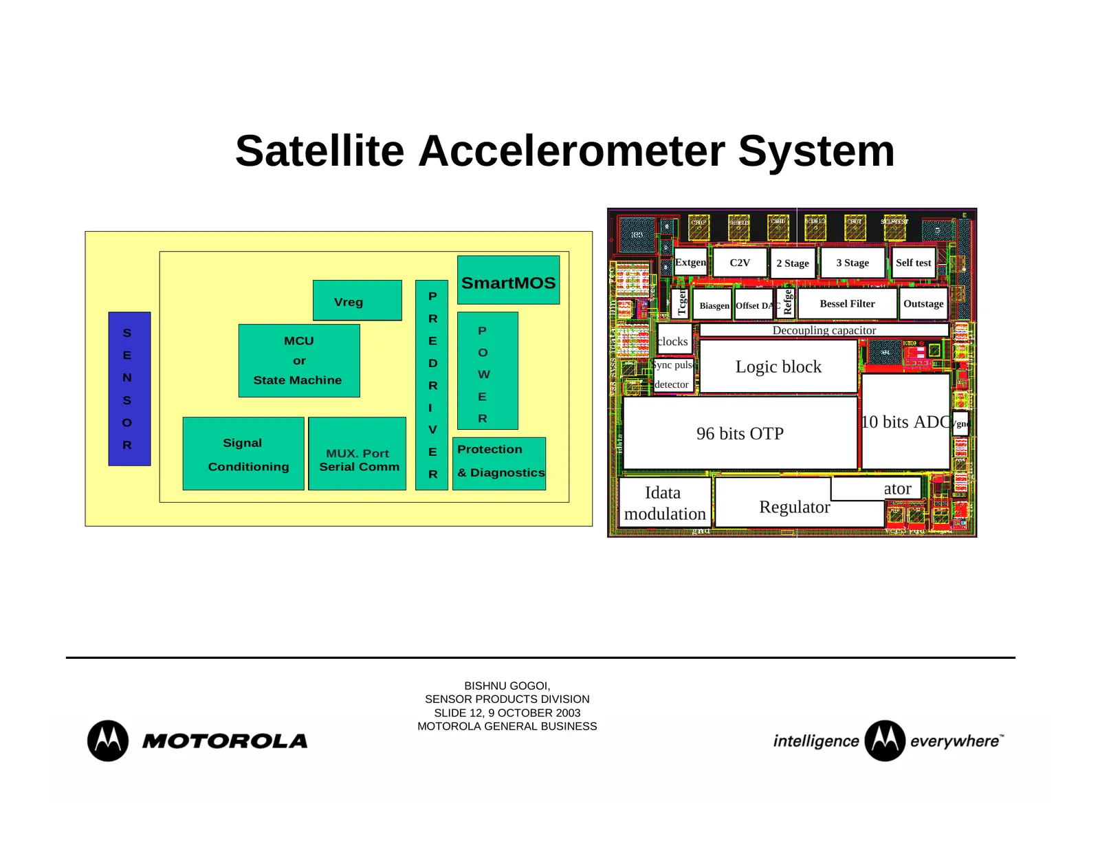
Slide 12: Satellite Accelerometer System
Satellite Accelerometer System Extgen C2V 2 Stage 3 Stage Self test SmartMOS Refgen Tcgen P Vreg Biasgen Offset DAC Bessel Filter Outstage R S P Decoupling capacitor MCU E clocks E O or D N W Sync pulse Logic block State Machine R detector S E I O R 10 bits ADCVgnd V Signal 96 bits OTP R Protection
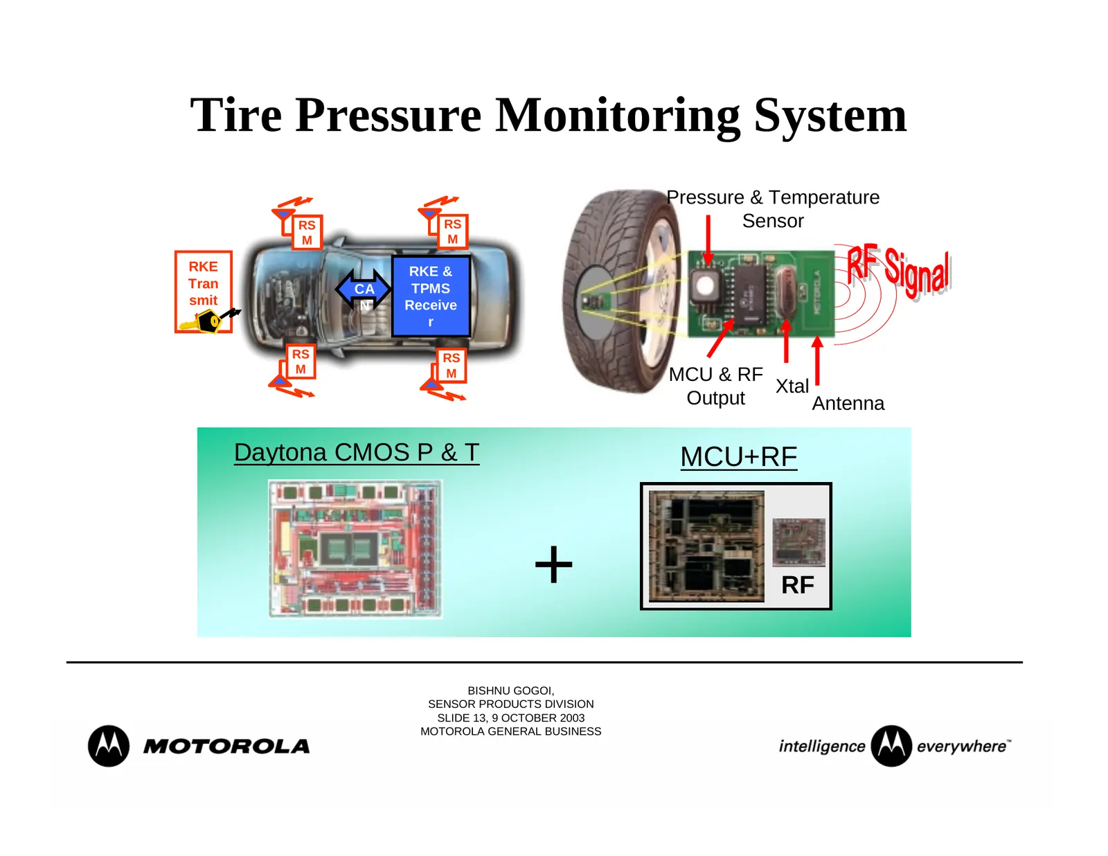
Slide 13: Tire Pressure Monitoring System
Tire Pressure Monitoring System Pressure & Temperature RS RS Sensor M M RKE RKE & Tran CA TPMS smit N Receive ter r RS RS M M MCU & RF Xtal Output Antenna Daytona CMOS P & T MCU+RF + RF BISHNU GOGOI, SENSOR PRODUCTS DIVISION SLIDE 13, 9 OCTOBER 2003 MOTOROLA GENERAL BUSINESS
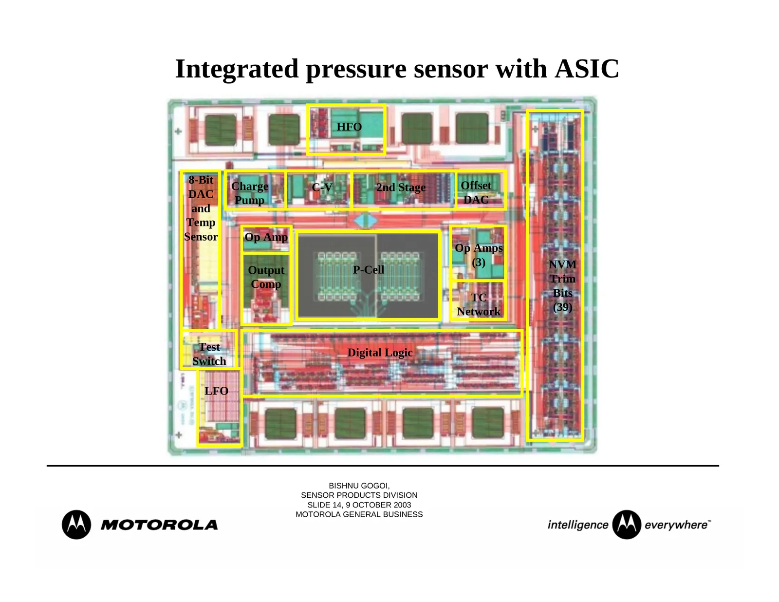
Slide 14: Integrated pressure sensor with ASIC
Integrated pressure sensor with ASIC HFO 8-Bit Offset Charge C-V 2nd Stage DAC DAC Pump and Temp Sensor Op Amp Op Amps (3) NVM Output P-Cell Comp Trim TC Bits Network (39) Test Digital Logic Switch LFO BISHNU GOGOI, SENSOR PRODUCTS DIVISION SLIDE 14, 9 OCTOBER 2003 MOTOROLA GENERAL BUSINESS
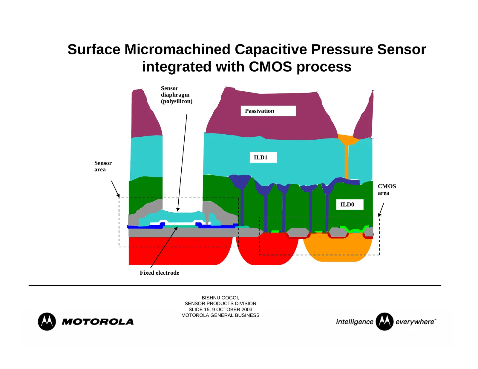
Slide 15: Surface Micromachined Capacitive Pressure Sensor integrated with CMOS process
Surface Micromachined Capacitive Pressure Sensor integrated with CMOS process Sensor diaphragm (polysilicon) Passivation ILD1 Sensor area CMOS area ILD0 Fixed electrode BISHNU GOGOI, SENSOR PRODUCTS DIVISION SLIDE 15, 9 OCTOBER 2003 MOTOROLA GENERAL BUSINESS
Slide 16: Function of a MEMS Package
Function of a MEMS Package • Protect Micro machined Structure through backend, module and end product manufacturing and end-use. • Facilitate Application System Level Assembly preferably using Automation • Provide Electrical Interface (Leads, Connectors etc.) • Provide Mechanical Interface (Support,
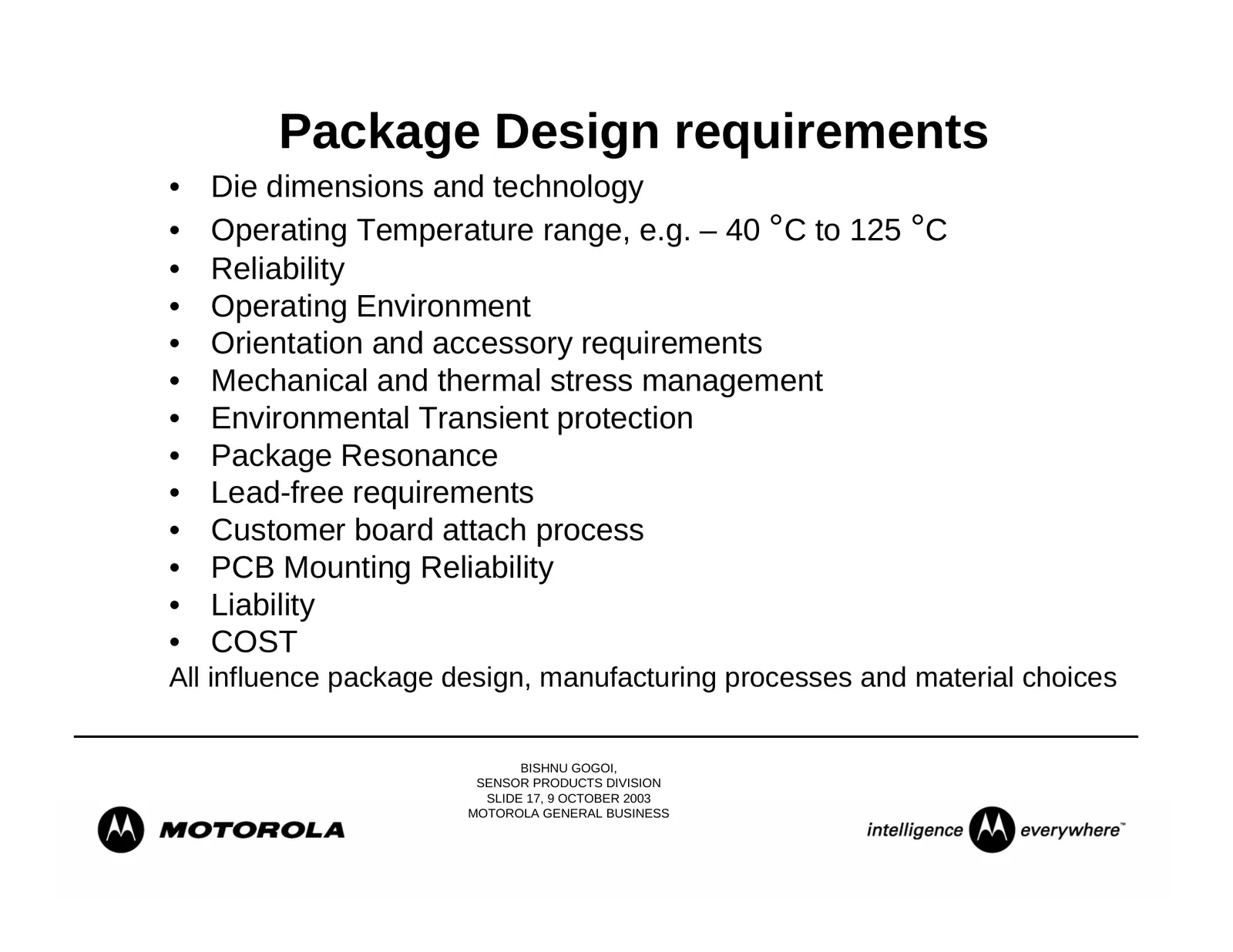
Slide 17: Package Design requirements
Package Design requirements • Die dimensions and technology • Operating Temperature range, e.g. – 40 °C to 125 °C • Reliability • Operating Environment • Orientation and accessory requirements • Mechanical and thermal stress management • Environmental Transient protection • Package Resonance • Lead-
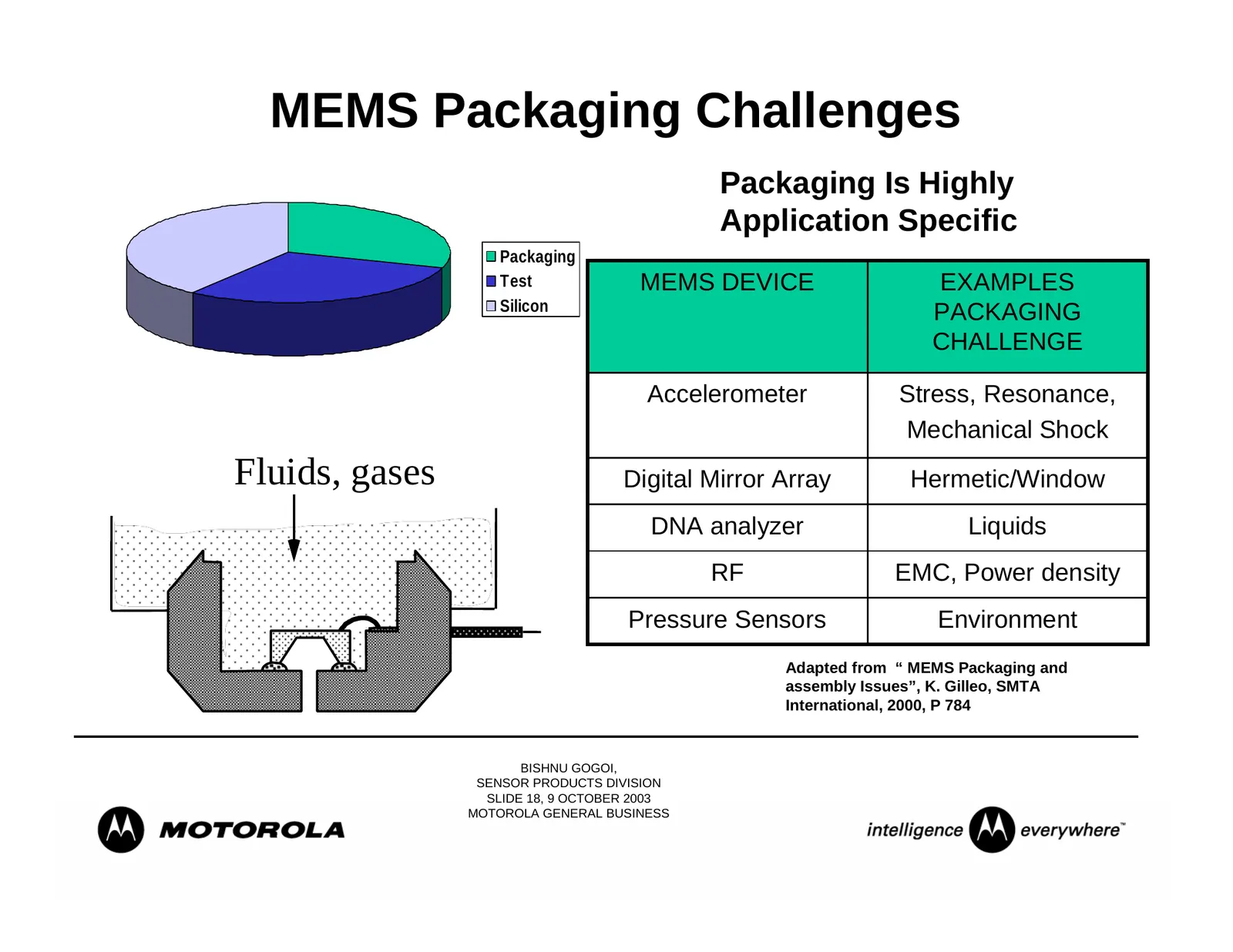
Slide 18: MEMS Packaging Challenges
MEMS Packaging Challenges Packaging Is Highly Application Specific Packaging Test MEMS DEVICE EXAMPLES Silicon PACKAGING CHALLENGE Accelerometer Stress, Resonance, Mechanical Shock Fluids, gases Digital Mirror Array Hermetic/Window DNA analyzer Liquids RF EMC, Power density Pressure Sensors Environm
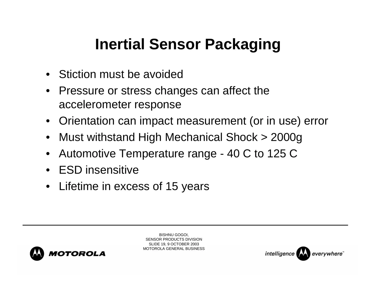
Slide 19: Inertial Sensor Packaging
Inertial Sensor Packaging • Stiction must be avoided • Pressure or stress changes can affect the accelerometer response • Orientation can impact measurement (or in use) error • Must withstand High Mechanical Shock > 2000g • Automotive Temperature range - 40 C to 125 C • ESD insensitive • Lifetime in
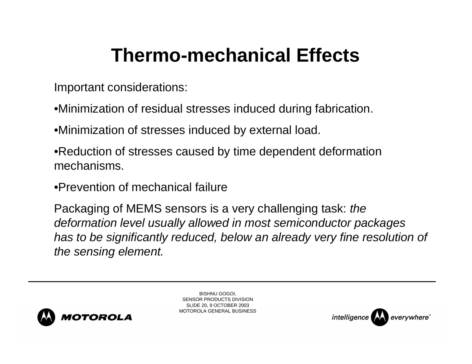
Slide 20: Thermo-mechanical Effects
Thermo-mechanical Effects Important considerations: •Minimization of residual stresses induced during fabrication. •Minimization of stresses induced by external load. •Reduction of stresses caused by time dependent deformation mechanisms. •Prevention of mechanical failure Packaging of MEMS sensors i
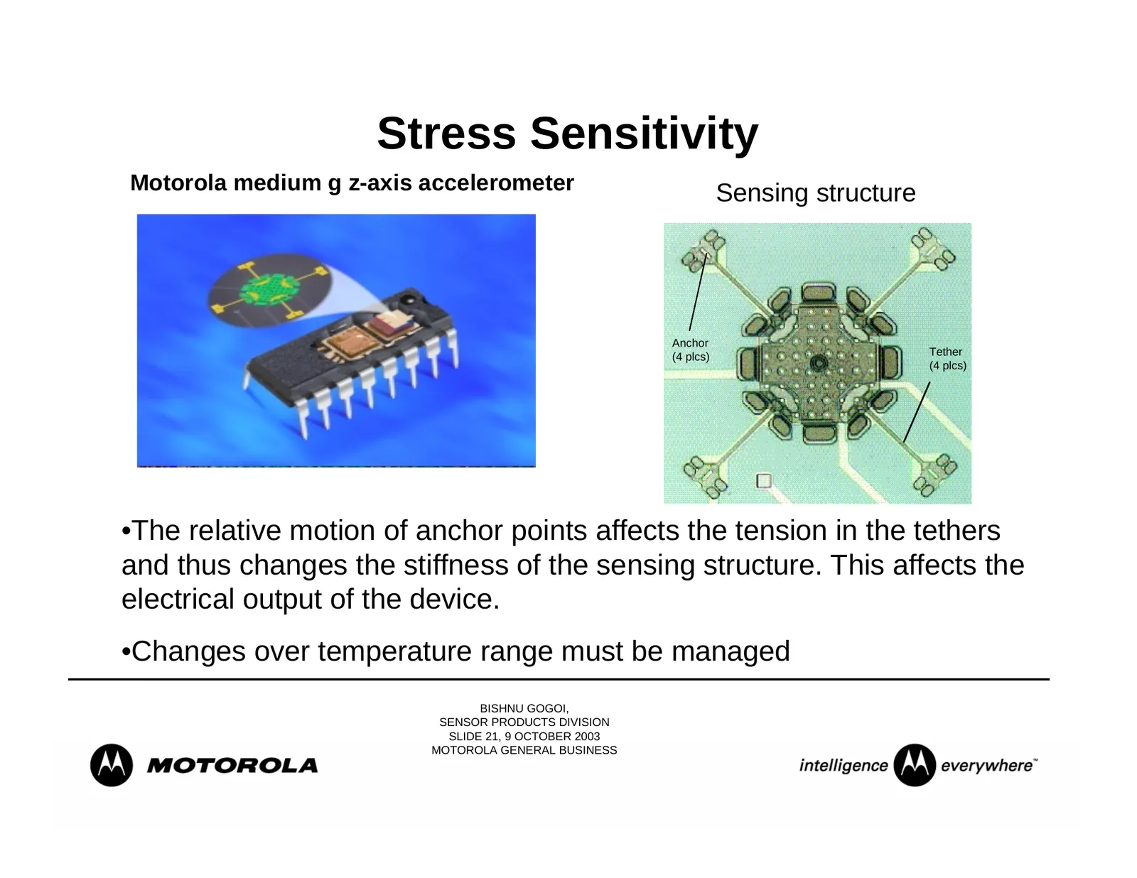
Slide 21: Stress Sensitivity
Stress Sensitivity Motorola medium g z-axis accelerometer Sensing structure Anchor (4 plcs) Tether (4 plcs) •The relative motion of anchor points affects the tension in the tethers and thus changes the stiffness of the sensing structure. This affects the electrical output of the device. •Changes ove
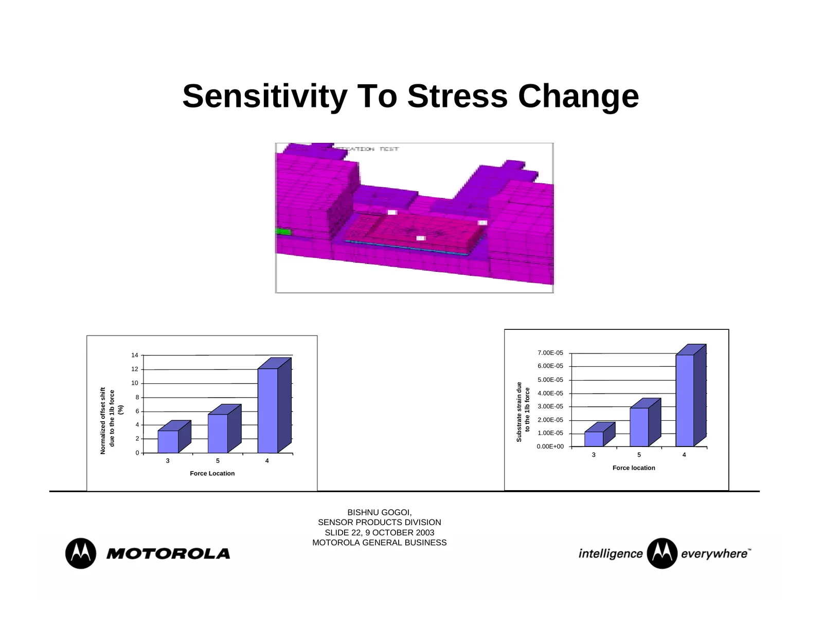
Slide 22: Sensitivity To Stress Change
Sensitivity To Stress Change 14 7.00E-05 6.00E-05 12 5.00E-05 10 Substrate strain due Normalized offset shift to the 1lb force due to the 1lb force 4.00E-05 8 3.00E-05 (%) 6 2.00E-05 4 1.00E-05 2 0.00E+00 0 3 5 4 3 5 4 Force location Force Location BISHNU GOGOI, SENSOR PRODUCTS DIVISION SLIDE 22, 9
Slide 23: Stress Management
Stress Management Objective: To design a system of silicon and package that overcomes the effects of sensor performance over changing environmental conditions. The Silicon and Package Designer must work cooperatively e.g. Material properties over temperature, environmental conditions, transducer des
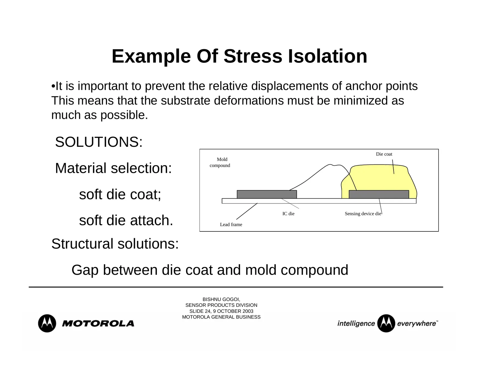
Slide 24: Example Of Stress Isolation
Example Of Stress Isolation •It is important to prevent the relative displacements of anchor points This means that the substrate deformations must be minimized as much as possible. SOLUTIONS: Die coat Mold Material selection: compound soft die coat; IC die Sensing device die soft die attach. Lead f
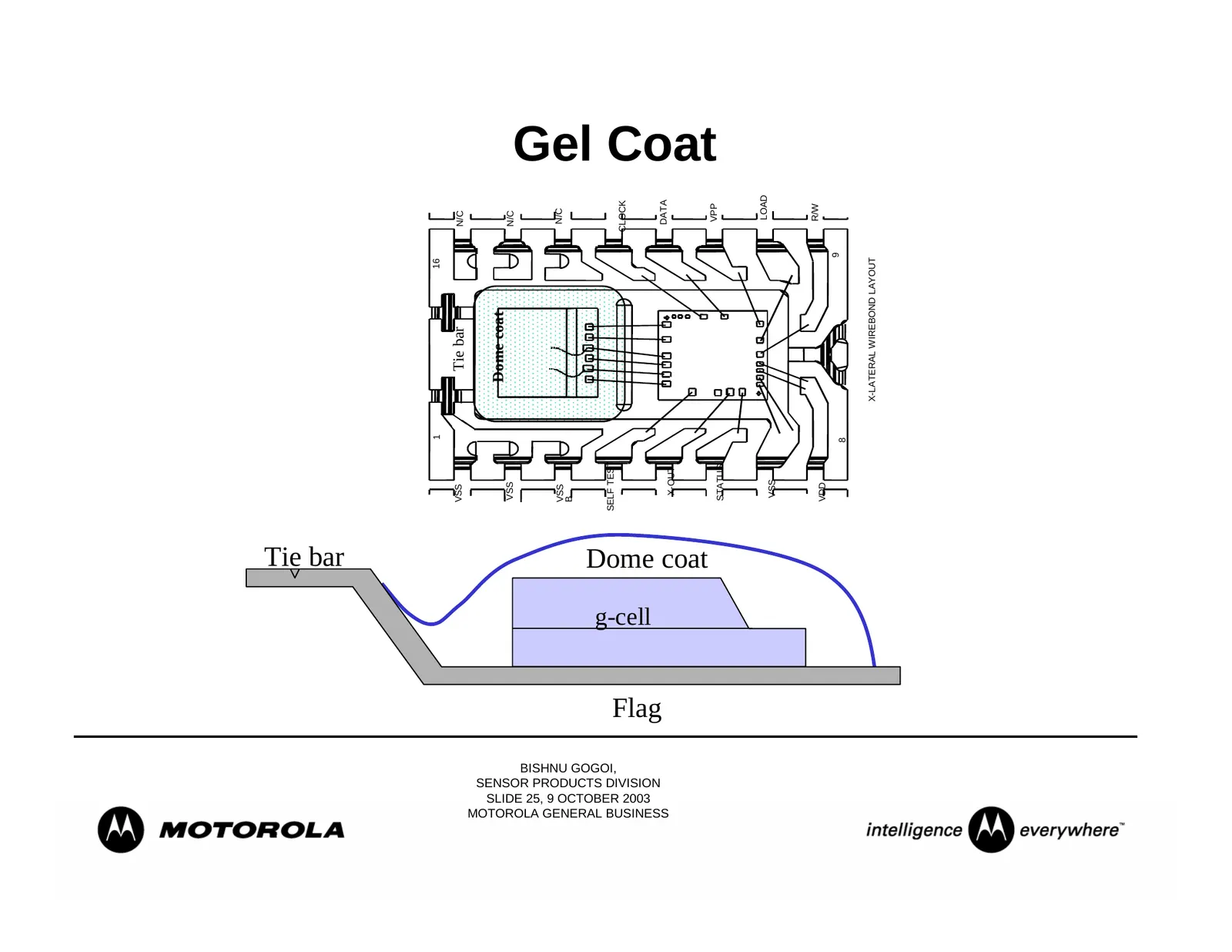
Slide 25: X-Lateral Wirebond Layout
Gel Coat LOAD CLOCK DATA VPP R/W N/C N/C N/C 9 X-LATERAL WIREBOND LAYOUT 16 Dome coat Tie bar 1 8 SELF TEST STATUS X-OUT VSS VSS VDD VSS VSS B Tie bar Dome coat g-cell Flag BISHNU GOGOI, SENSOR PRODUCTS DIVISION SLIDE 25, 9 OCTOBER 2003 MOTOROLA GENERAL BUSINESS
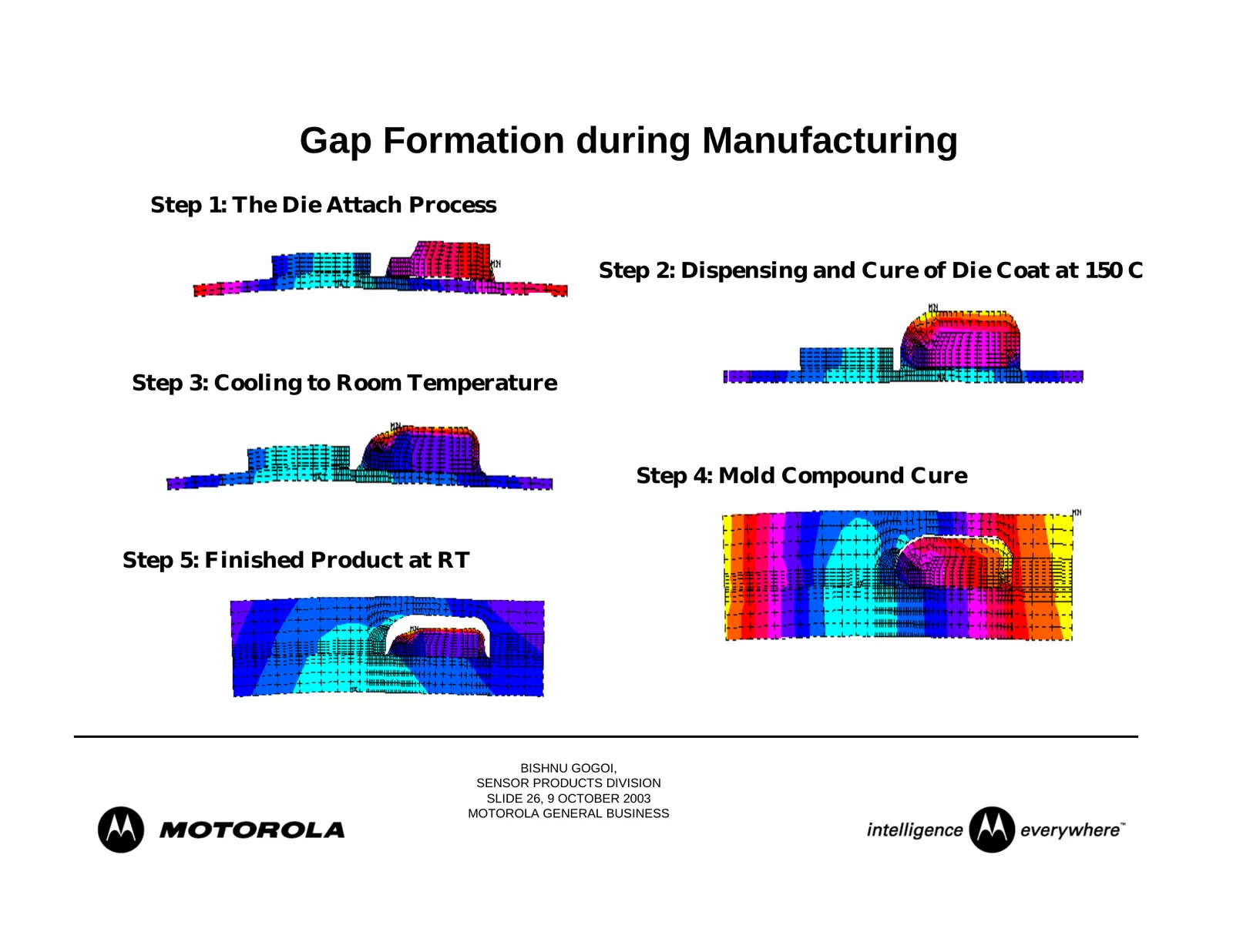
Slide 26: Gap Formation during Manufacturing
Gap Formation during Manufacturing Step 1: The Die Attach Process Step 2: Dispensing and Cure of Die Coat at 150 C Step 3: Cooling to Room Temperature Step 4: Mold Compound Cure Step 5: Finished Product at RT BISHNU GOGOI, SENSOR PRODUCTS DIVISION SLIDE 26, 9 OCTOBER 2003 MOTOROLA GENERAL BUSINESS
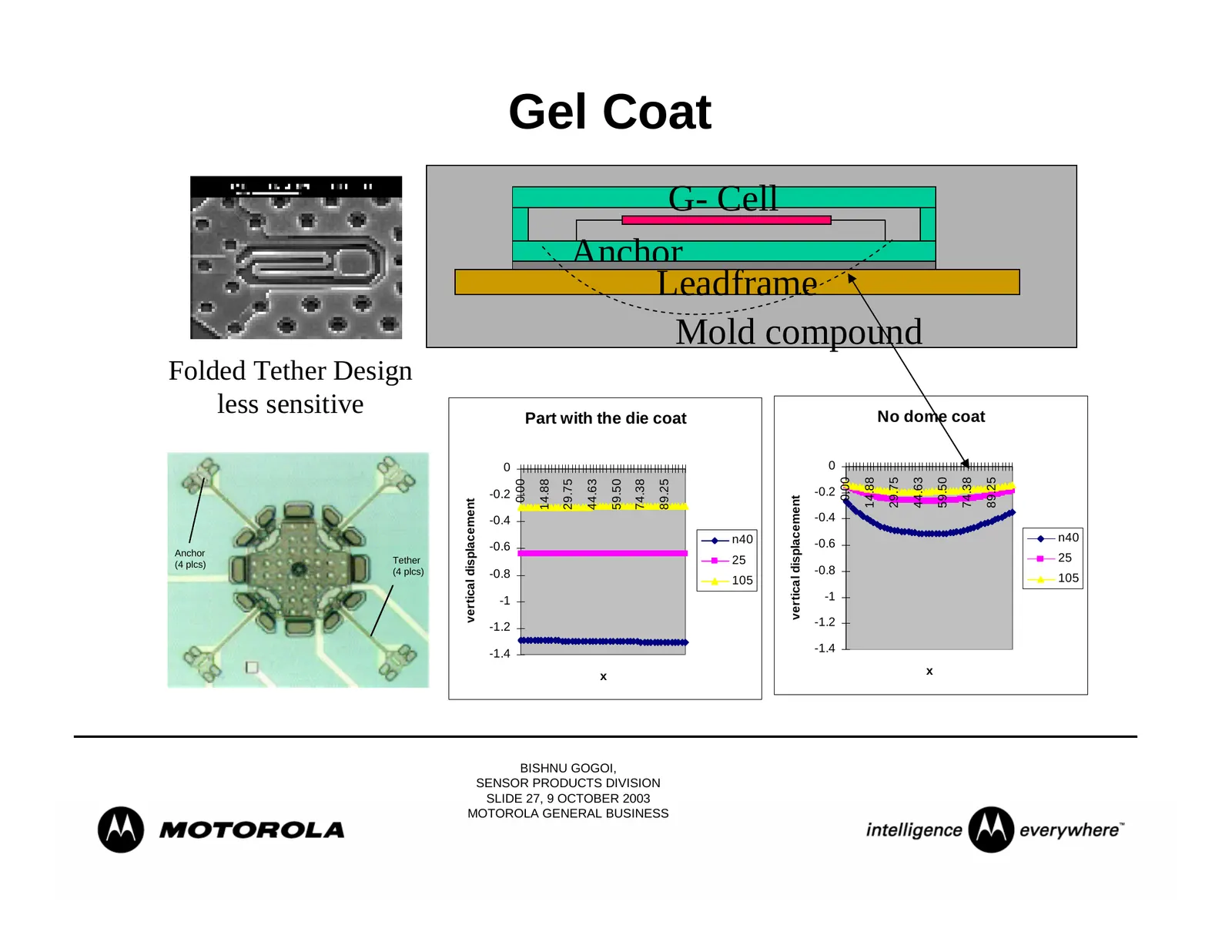
Slide 27: Vertical displacement
Gel Coat G- Cell Anchor Leadframe Mold compound Folded Tether Design less sensitive Part with the die coat No dome coat 0 0 0.00 14.88 29.75 44.63 59.50 74.38 89.25 0.00 14.88 29.75 44.63 59.50 74.38 89.25 -0.2 -0.2 vertical displacement vertical displacement -0.4 -0.4 n40 n40 -0.6 -0.6 Anchor (4 pl
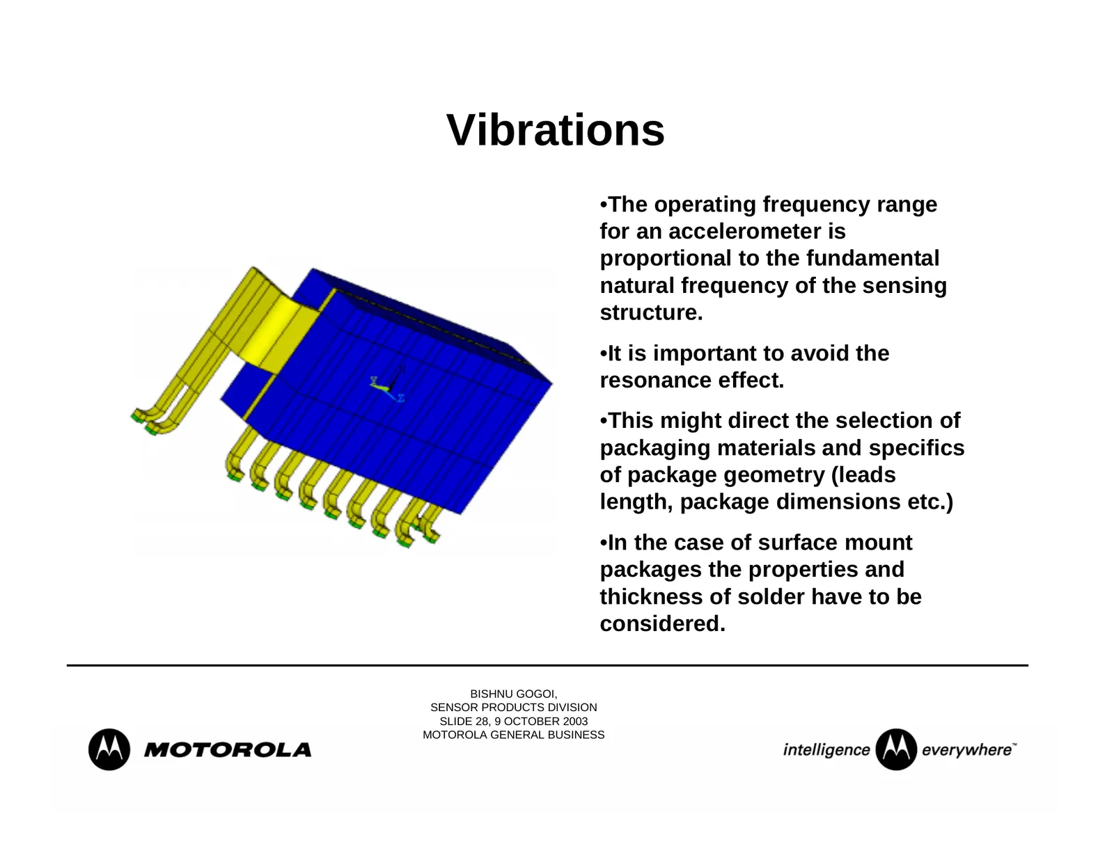
Slide 28: Vibrations
Vibrations •The operating frequency range for an accelerometer is proportional to the fundamental natural frequency of the sensing structure. •It is important to avoid the resonance effect. •This might direct the selection of packaging materials and specifics of package geometry (leads length, packa
Slide 29: Design Methods and Theoretical Models
Design Methods and Theoretical Models • Design process for MEMS packages incorporates standard tools and methods (experimental, numerical, and analytical) used in the design of IC packages. • MEMS packaging faces similar problems as IC packaging: the absence of theoretical models • The development o
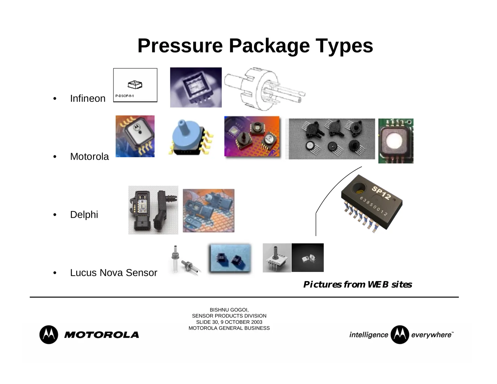
Slide 30: Pressure Package Types
Pressure Package Types • Infineon • Motorola • Delphi • Lucus Nova Sensor Pictures from WEB sites BISHNU GOGOI, SENSOR PRODUCTS DIVISION SLIDE 30, 9 OCTOBER 2003 MOTOROLA GENERAL BUSINESS
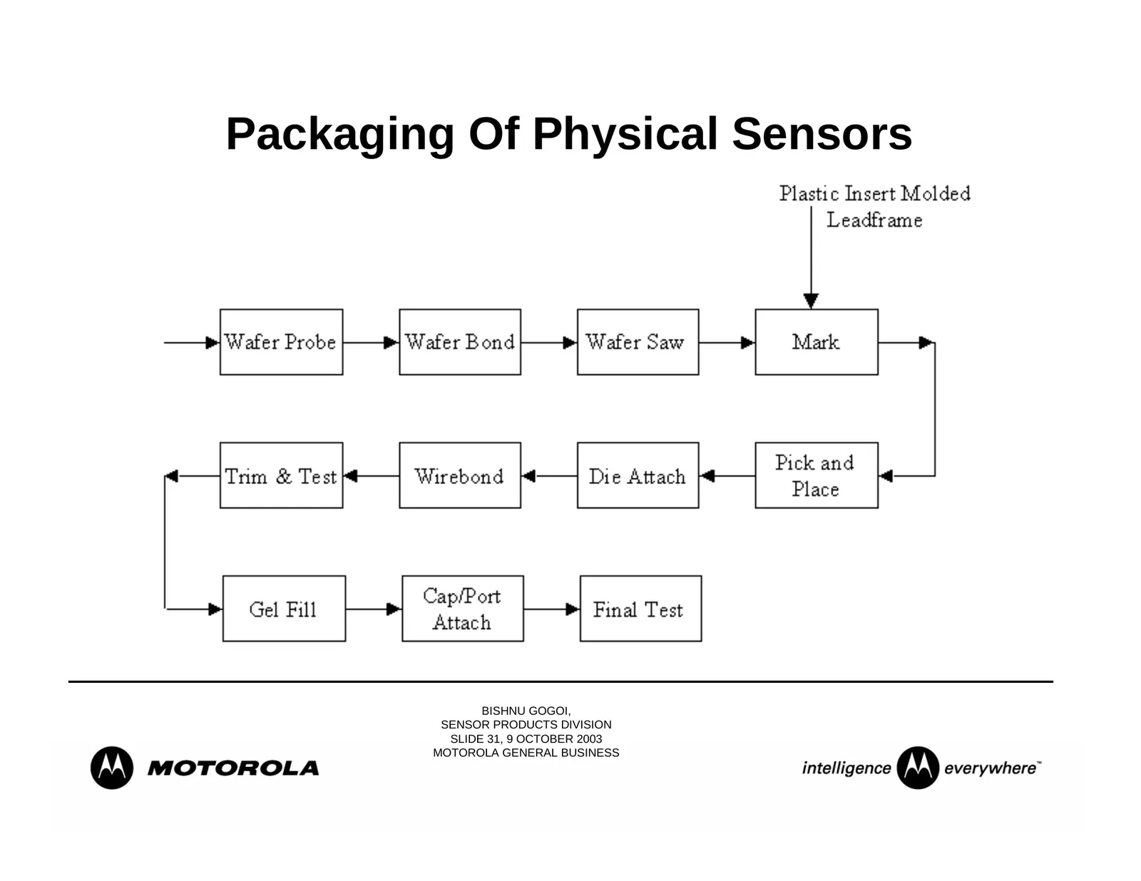
Slide 31: Packaging Of Physical Sensors
Packaging Of Physical Sensors BISHNU GOGOI, SENSOR PRODUCTS DIVISION SLIDE 31, 9 OCTOBER 2003 MOTOROLA GENERAL BUSINESS
Slide 32: Pressure Sensor Packaging Issues
Pressure Sensor Packaging Issues • Small material usage • Understanding of interactions among packaging materials, induced stress and device performance • Measurements of material properties for all packaging materials • Lot-to-lot variability of some materials • Modeling accuracy for the behavior o
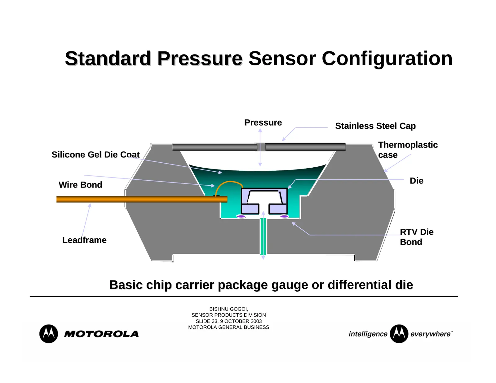
Slide 33: Standard Pressure Sensor Configuration
Standard Pressure Sensor Configuration Pressure Stainless Steel Cap Thermoplastic Silicone Gel Die Coat case Wire Bond Die RTV Die Leadframe Bond Pressure Basic chip carrier package gauge or differential die BISHNU GOGOI, SENSOR PRODUCTS DIVISION SLIDE 33, 9 OCTOBER 2003 MOTOROLA GENERAL BUSINESS
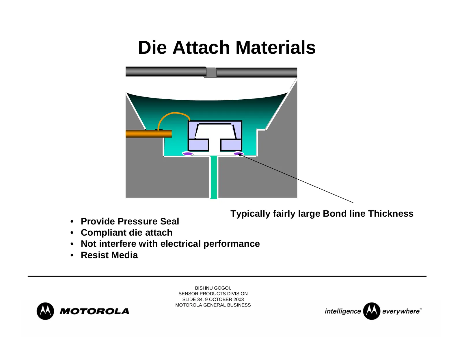
Slide 34: Die Attach Materials
Die Attach Materials Pressure Typically fairly large Bond line Thickness • Provide Pressure Seal • Compliant die attach • Not interfere with electrical performance • Resist Media BISHNU GOGOI, SENSOR PRODUCTS DIVISION SLIDE 34, 9 OCTOBER 2003 MOTOROLA GENERAL BUSINESS
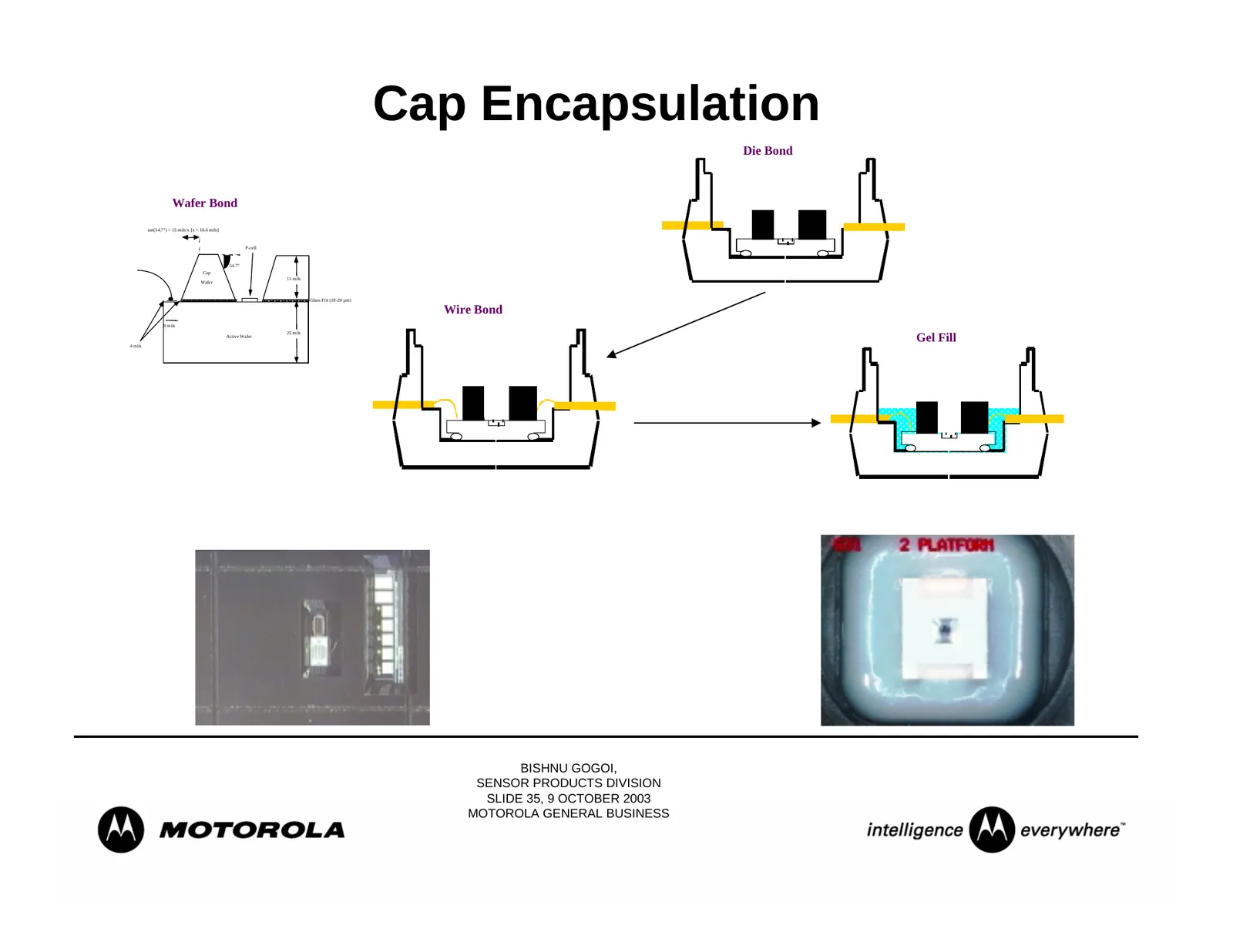
Slide 35: Cap Encapsulation
Cap Encapsulation Die Bond Wafer Bond tan(54.7°) = 15 mils/x [x = 10.6 mils] P-cell 54.7° Cap 15 mils Wafer Glass Frit (10-20 µm) Wire Bond 8 mils 25 mils Active Wafer Gel Fill 4 mils BISHNU GOGOI, SENSOR PRODUCTS DIVISION SLIDE 35, 9 OCTOBER 2003 MOTOROLA GENERAL BUSINESS
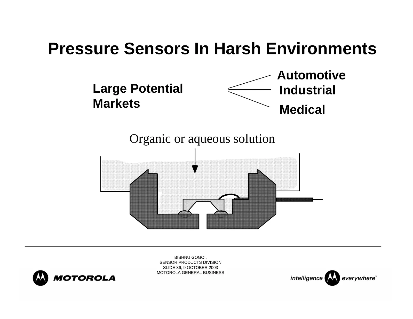
Slide 36: Pressure Sensors In Harsh Environments
Pressure Sensors In Harsh Environments Automotive Large Potential Industrial Markets Medical Organic or aqueous solution BISHNU GOGOI, SENSOR PRODUCTS DIVISION SLIDE 36, 9 OCTOBER 2003 MOTOROLA GENERAL BUSINESS
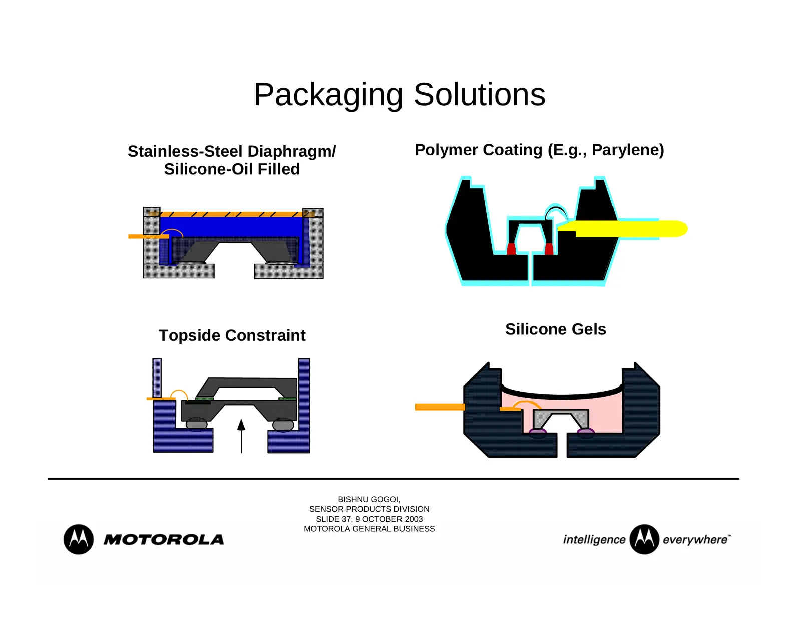
Slide 37: Packaging Solutions
Packaging Solutions Stainless-Steel Diaphragm/ Polymer Coating (E.g., Parylene) Silicone-Oil Filled Topside Constraint Silicone Gels BISHNU GOGOI, SENSOR PRODUCTS DIVISION SLIDE 37, 9 OCTOBER 2003 MOTOROLA GENERAL BUSINESS
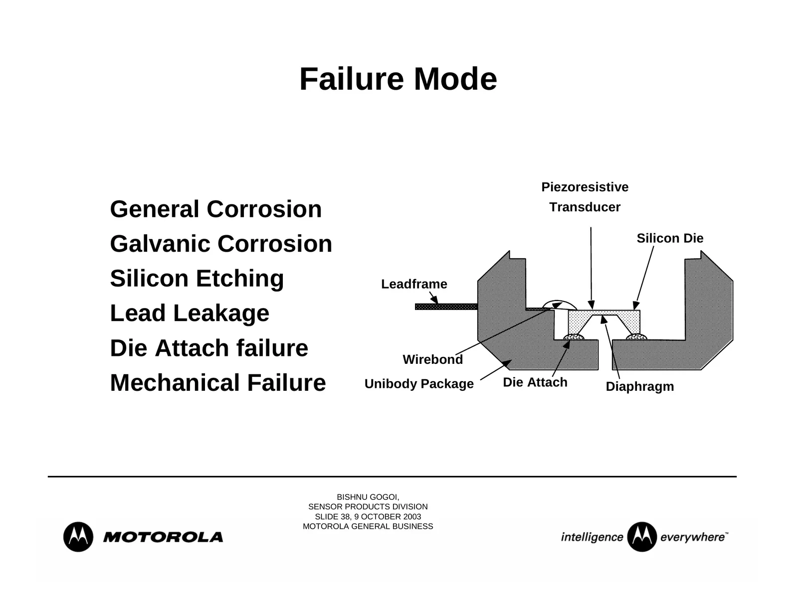
Slide 38: Failure Mode
Failure Mode Piezoresistive General Corrosion Transducer Silicon Die Galvanic Corrosion Silicon Etching Leadframe Lead Leakage Die Attach failure Wirebond Mechanical Failure Unibody Package Die Attach Diaphragm BISHNU GOGOI, SENSOR PRODUCTS DIVISION SLIDE 38, 9 OCTOBER 2003 MOTOROLA GENERAL BUSINESS
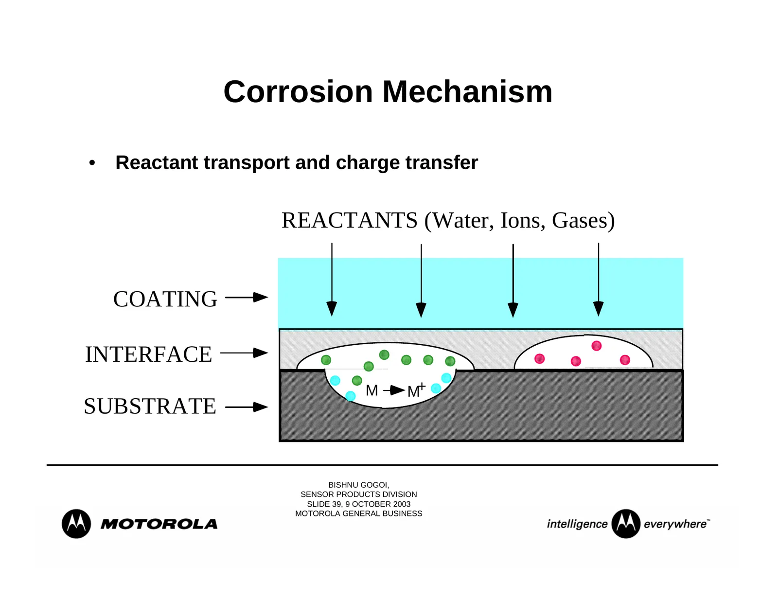
Slide 39: Corrosion Mechanism
Corrosion Mechanism • Reactant transport and charge transfer REACTANTS (Water, Ions, Gases) COATING INTERFACE M M+ SUBSTRATE BISHNU GOGOI, SENSOR PRODUCTS DIVISION SLIDE 39, 9 OCTOBER 2003 MOTOROLA GENERAL BUSINESS
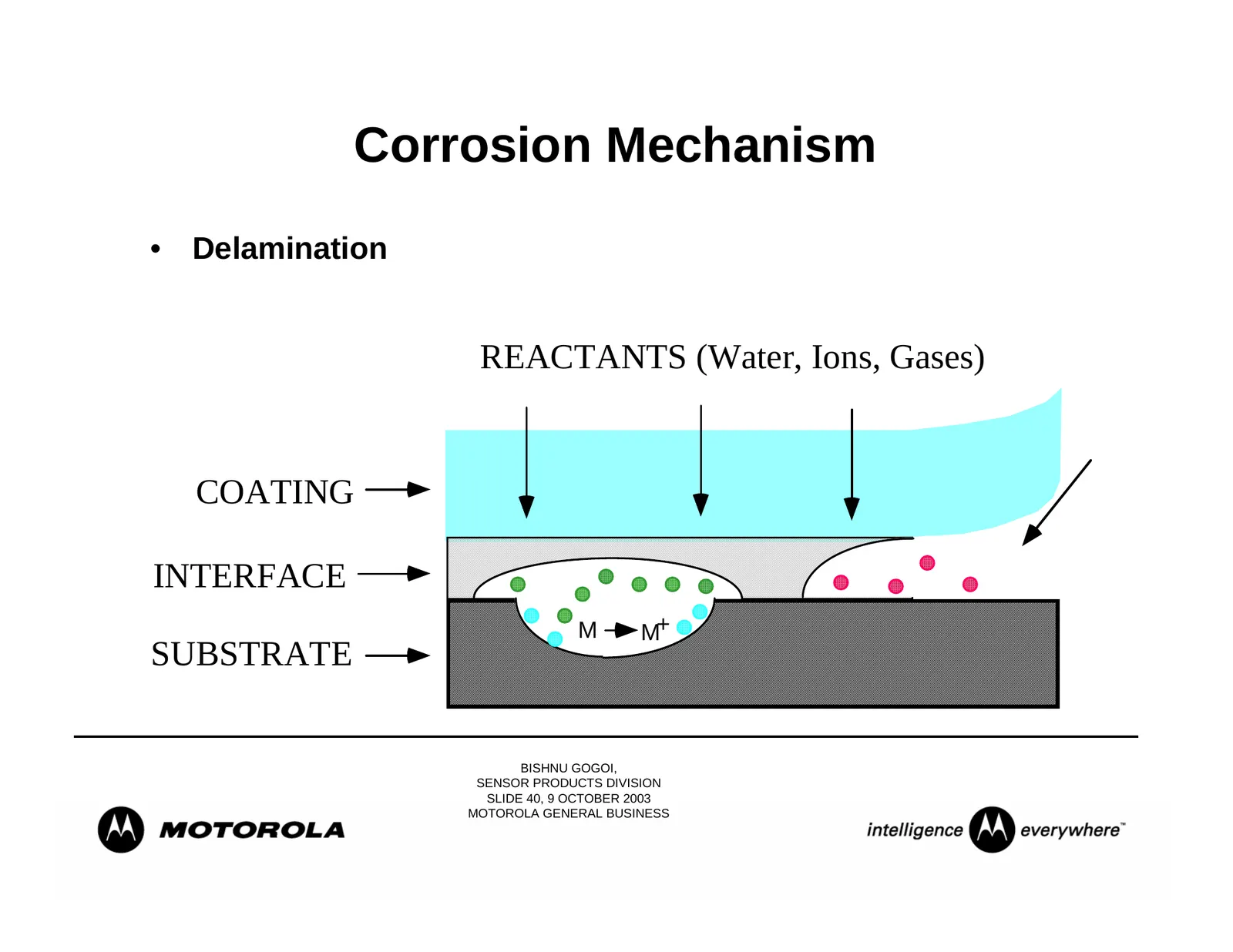
Slide 40: Corrosion Mechanism
Corrosion Mechanism • Delamination REACTANTS (Water, Ions, Gases) COATING INTERFACE M M+ SUBSTRATE BISHNU GOGOI, SENSOR PRODUCTS DIVISION SLIDE 40, 9 OCTOBER 2003 MOTOROLA GENERAL BUSINESS
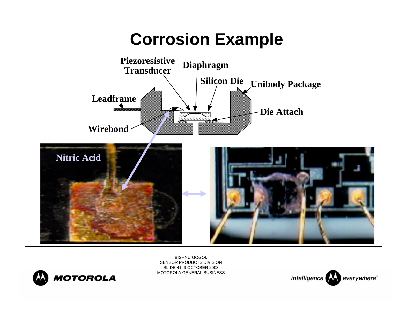
Slide 41: Corrosion Example
Corrosion Example Piezoresistive Diaphragm Transducer Silicon Die Unibody Package Leadframe Die Attach Wirebond Nitric Acid BISHNU GOGOI, SENSOR PRODUCTS DIVISION SLIDE 41, 9 OCTOBER 2003 MOTOROLA GENERAL BUSINESS
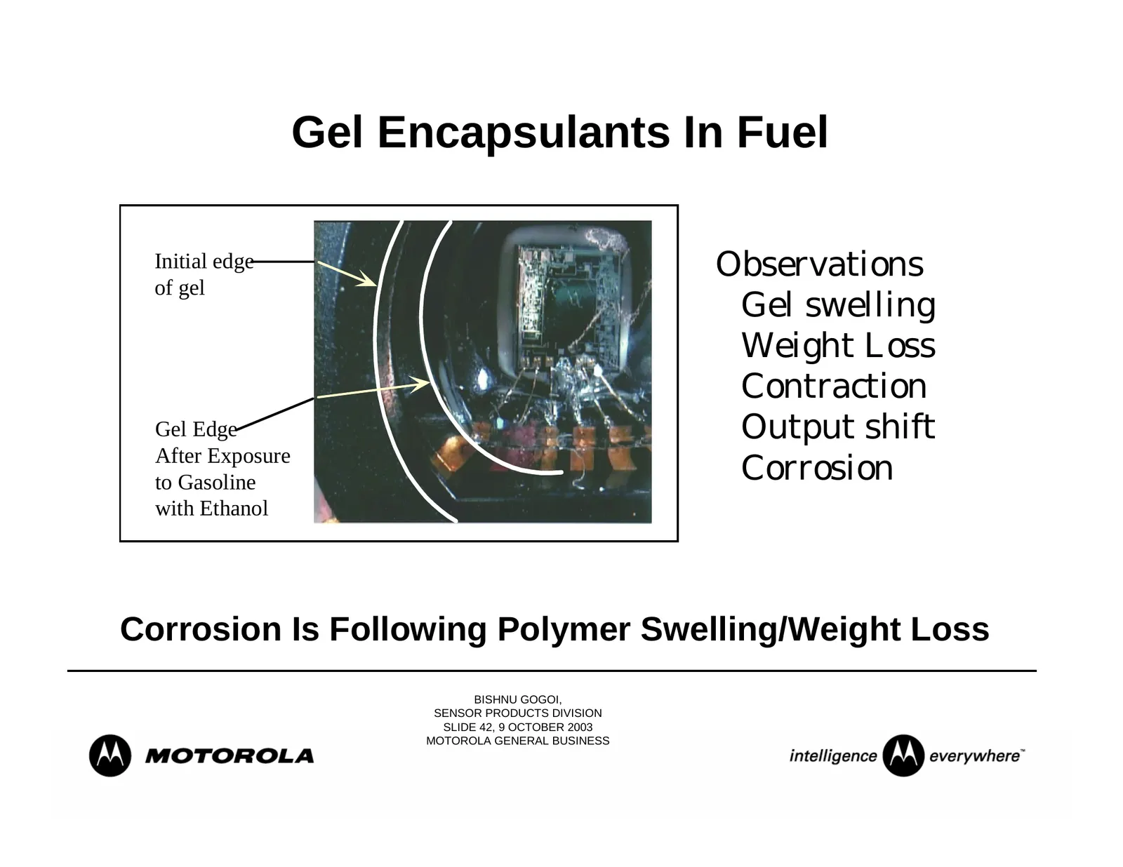
Slide 42: Gel Encapsulants In Fuel
Gel Encapsulants In Fuel Initial edge Observations of gel Gel swelling Weight Loss Contraction Gel Edge Output shift After Exposure to Gasoline Corrosion with Ethanol Corrosion Is Following Polymer Swelling/Weight Loss BISHNU GOGOI, SENSOR PRODUCTS DIVISION SLIDE 42, 9 OCTOBER 2003 MOTOROLA GENERAL
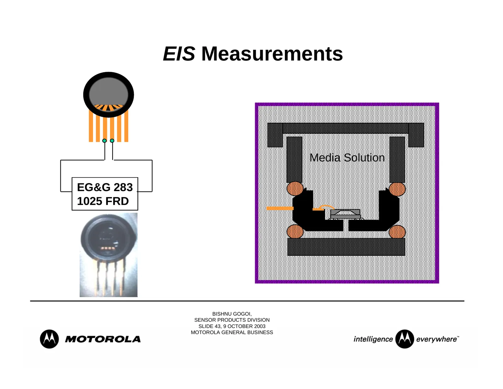
Slide 43: EIS Measurements
EIS Measurements Media Solution EG&G 283 1025 FRD BISHNU GOGOI, SENSOR PRODUCTS DIVISION SLIDE 43, 9 OCTOBER 2003 MOTOROLA GENERAL BUSINESS
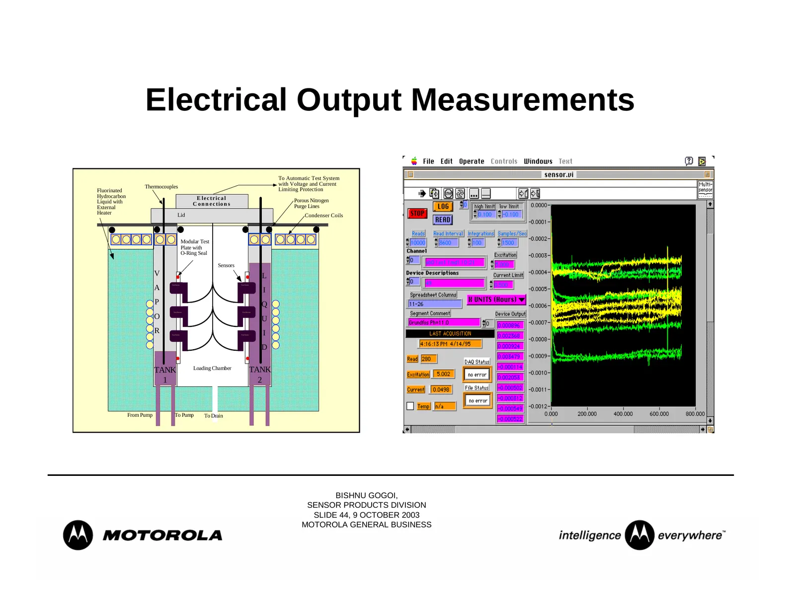
Slide 44: Electrical Output Measurements
Electrical Output Measurements To Automatic Test System with Voltage and Current Thermocouples Limiting Protection Fluorinated Hydrocarbon E le c tric a l Liquid with Porous Nitrogen C o n n e c tio n s Purge Lines External Heater Lid Condenser Coils Modular Test Plate with O-Ring Seal Sensors V L T
Slide 45: Fuel Exposure Experiment
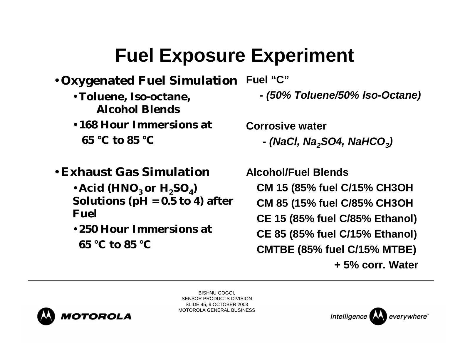
Fuel Exposure Experiment •Oxygenated Fuel Simulation Fuel “C” •Toluene, Iso-octane, - (50% Toluene/50% Iso-Octane) Alcohol Blends •168 Hour Immersions at Corrosive water 65 °C to 85 °C - (NaCl, Na2SO4, NaHCO3) •Exhaust Gas Simulation Alcohol/Fuel Blends •Acid (HNO3 or H2SO4) CM 15 (85% fuel C/15% CH
Slide 46: Wafer level packaging
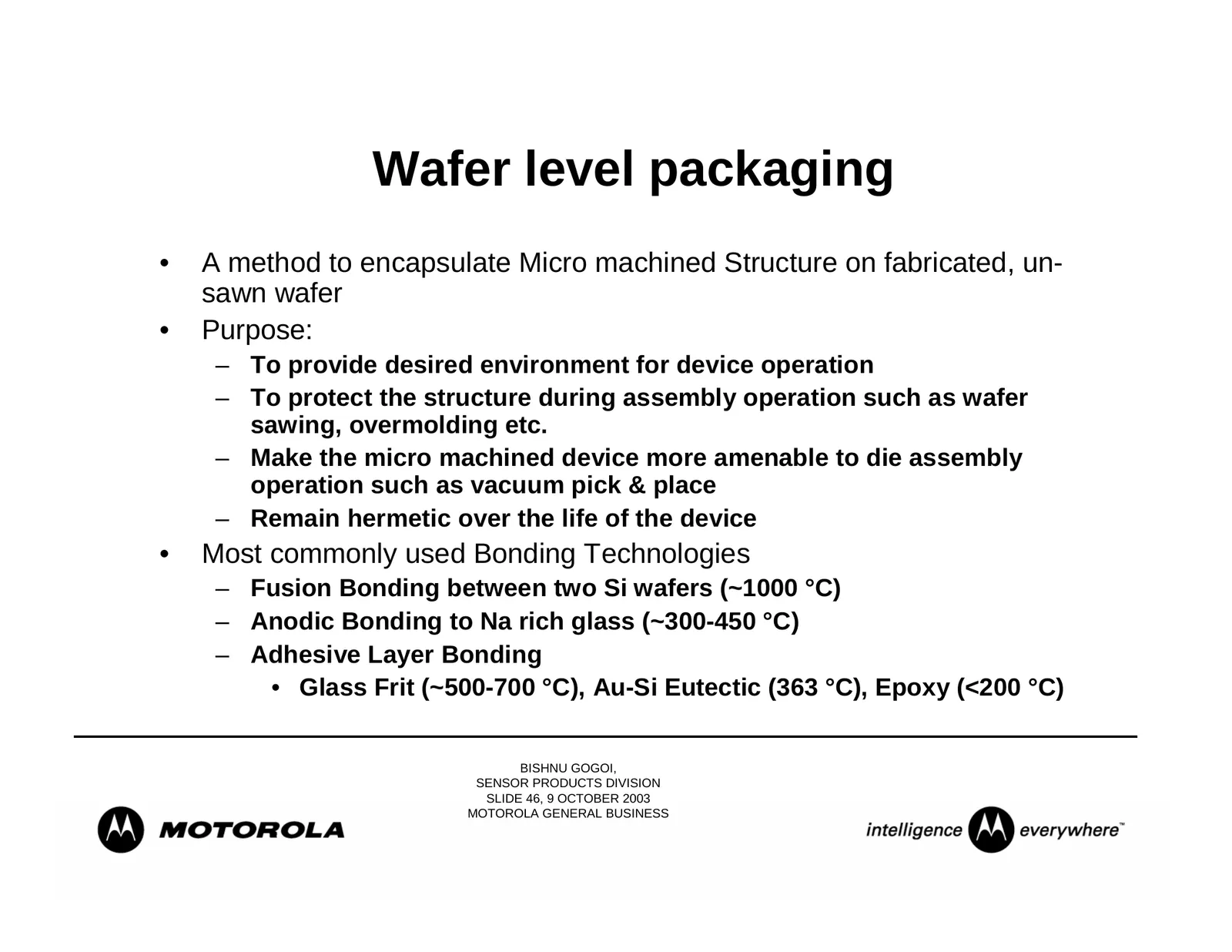
Wafer level packaging • A method to encapsulate Micro machined Structure on fabricated, un- sawn wafer • Purpose: – To provide desired environment for device operation – To protect the structure during assembly operation such as wafer sawing, overmolding etc. – Make the micro machined device more am
Slide 47: Wafer Bonding
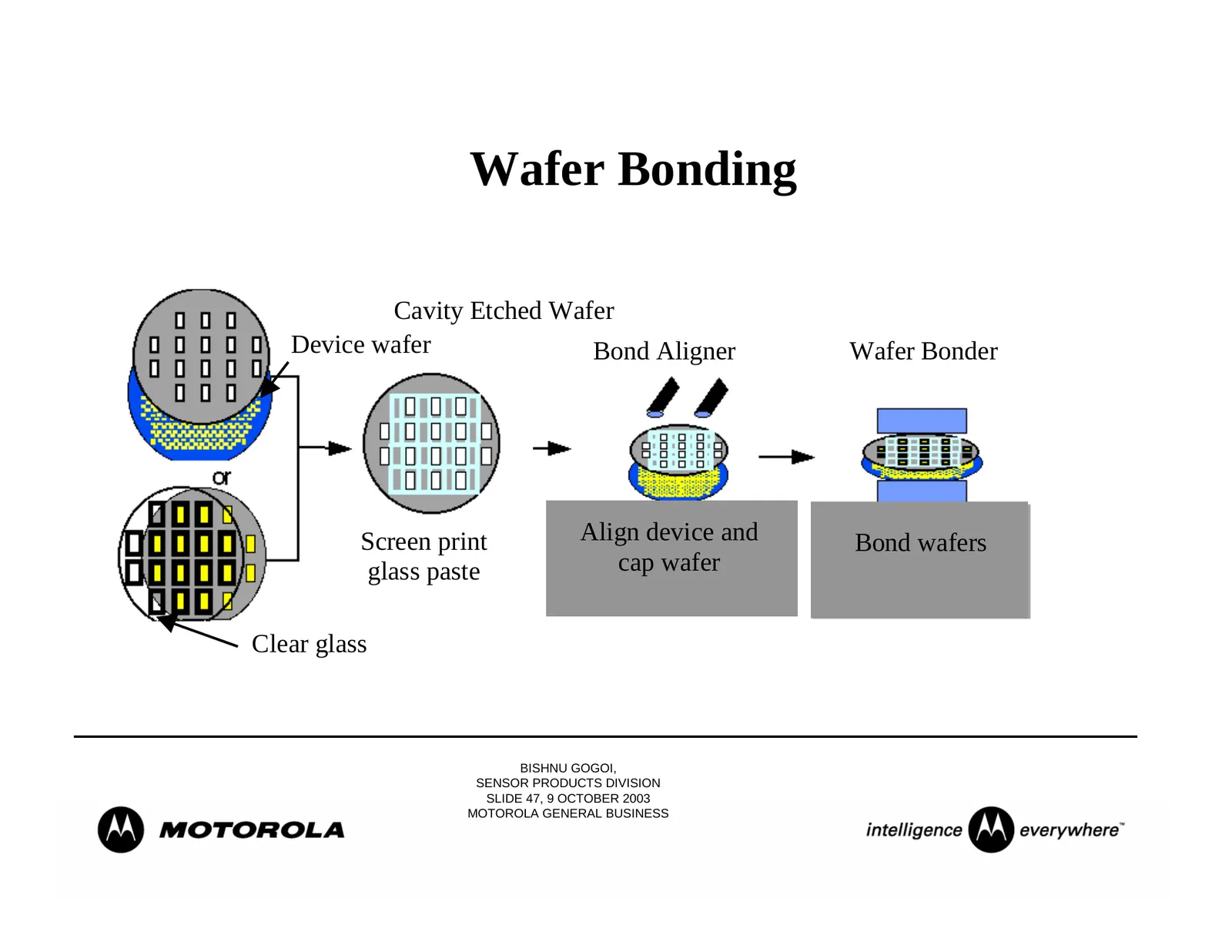
Wafer Bonding Cavity Etched Wafer Device wafer Bond Aligner Wafer Bonder Screen print Align device and Bond wafers glass paste cap wafer Clear glass BISHNU GOGOI, SENSOR PRODUCTS DIVISION SLIDE 47, 9 OCTOBER 2003 MOTOROLA GENERAL BUSINESS
Slide 48: Wafer Level Packaging
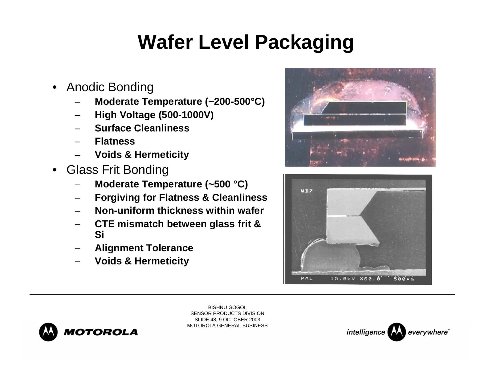
Wafer Level Packaging • Anodic Bonding – Moderate Temperature (~200-500°C) – High Voltage (500-1000V) – Surface Cleanliness – Flatness – Voids & Hermeticity • Glass Frit Bonding – Moderate Temperature (~500 °C) – Forgiving for Flatness & Cleanliness – Non-uniform thickness within wafer – CTE mismatc
Slide 49: Summary
Summary • High volume MEMS sensors using surface and bulk micromachining are proliferating in many application areas • The challenges for MEMS packaging are application specific • The trend for microsystem technology is for higher levels of integration • Need to leverage existing manufacturing techn

Slide 50: Acknowledgements
Acknowledgements Mike Chapman Slobodan Petrovic Milena Vujosevic Gary Li Mike Cheperak Raj Verma Tom Hatfield Dragan Mladenovic BISHNU GOGOI, SENSOR PRODUCTS DIVISION SLIDE 50, 9 OCTOBER 2003 MOTOROLA GENERAL BUSINESS
Source: Internet Archive copy of suss.com
More decks from SUSS MicroTec SE
 9M 2026 Earnings Presentation23 slides · Nov 5, 2026
 Investor Presentation (October 2026)41 slides · October 2026
 H1 2026 Earnings Presentation24 slides · Aug 6, 2026
 Q1 2026 Earnings Presentation19 slides · May 7, 2026
 FY2025 Earnings Presentation26 slides · Mar 30, 2026
 Investor Presentation (March 2026)42 slides · Mar 1, 2026