AAC Clyde Space AB · OMXSTO:AAC
AAC Clyde Space AB — Ångström Aerospace — Technical Presentation (2008)
24 slides from AAC Clyde Space AB's technical presentation, 2008
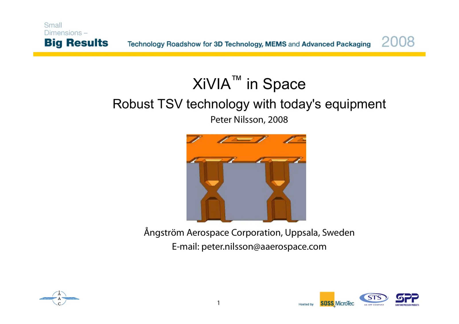
Slide 1: XiVIA in Space
XiVIA™ in Space Robust TSV technology with today's equipment Peter Nilsson, 2008 Ångström Aerospace Corporation, Uppsala, Sweden E-mail: peter.nilsson@aaerospace.com 1
Slide 2: Ångström Aerospace Corporation (ÅAC)
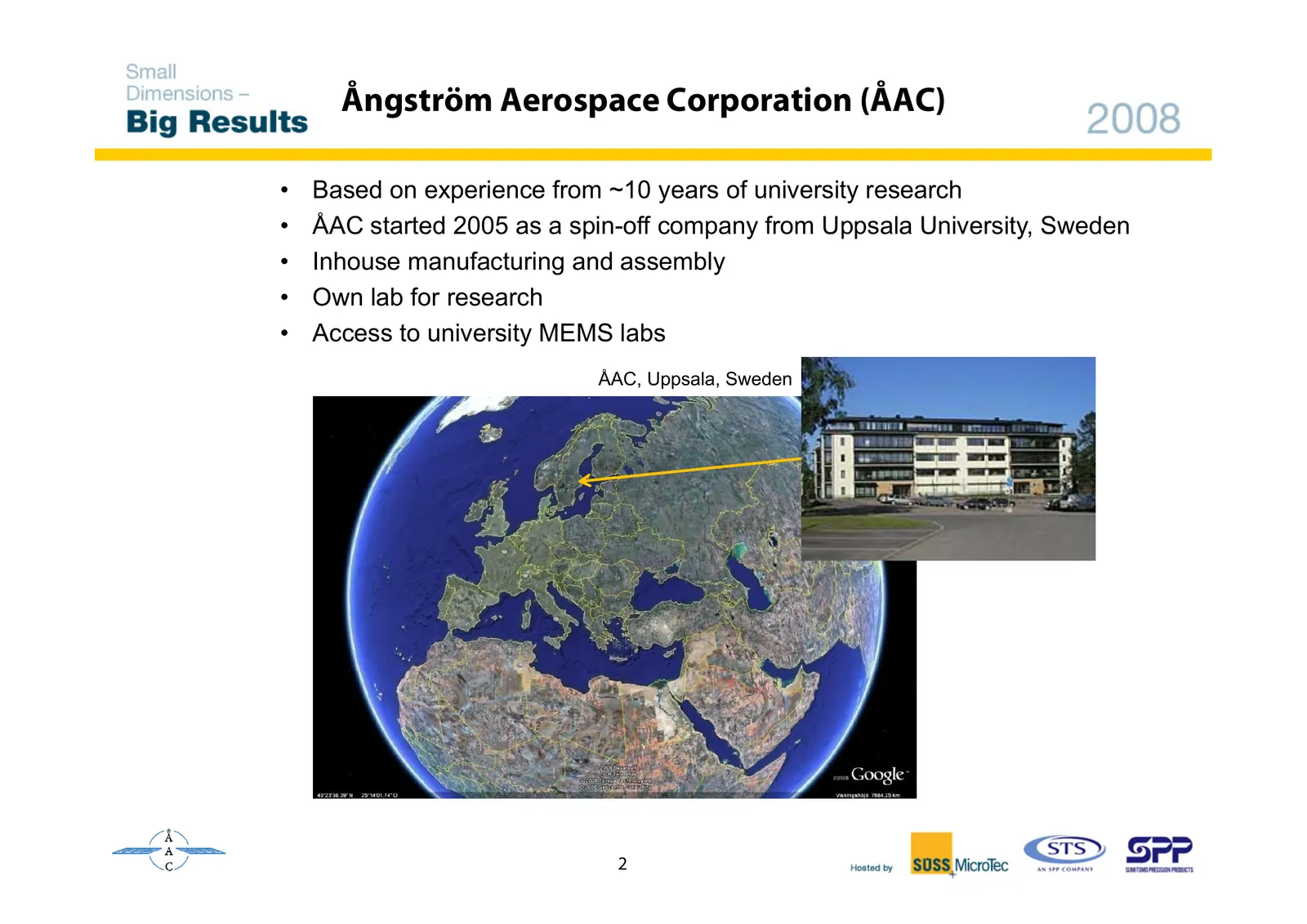
Ångström Aerospace Corporation (ÅAC) • Based on experience from ~10 years of university research • ÅAC started 2005 as a spin-off company from Uppsala University, Sweden • I h Inhouse manufacturing f i andd assembly bl • Own lab for research • Access to university MEMS labs ÅAC, Uppsala, Sweden 2
Slide 3: Ångström Aerospace Corporation (ÅAC)
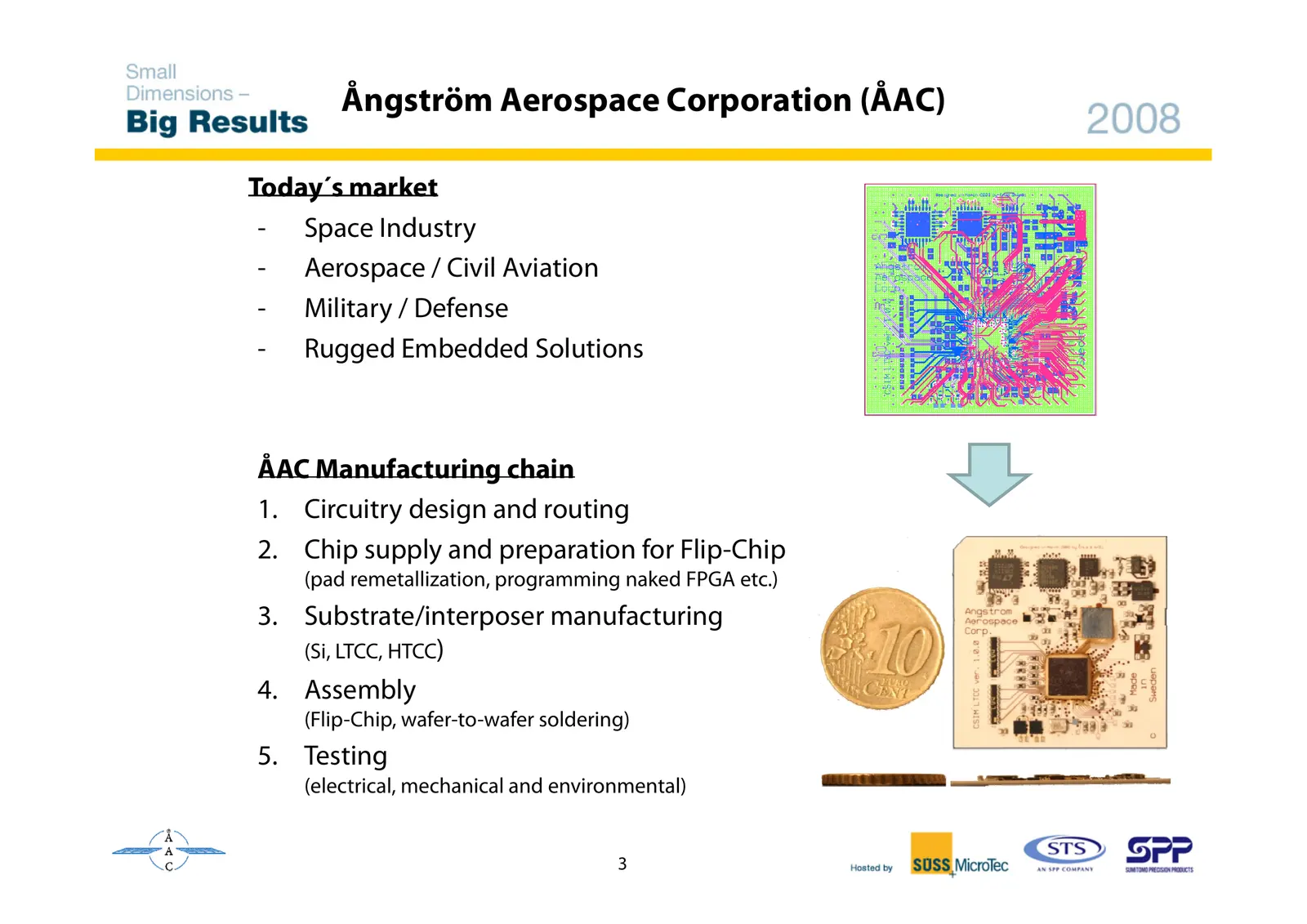
Ångström Aerospace Corporation (ÅAC) Today´s market - Space Industry - Aerospace / Civil Aviation - Military / Defense - Rugged Embedded Solutions ÅAC Manufacturing M f t i chainh i 1. Circuitry design and routing 2. Chip supply and preparation for Flip-Chip (pad remetallization, programming naked F
Slide 4: Reduction of Form Factor by Integration
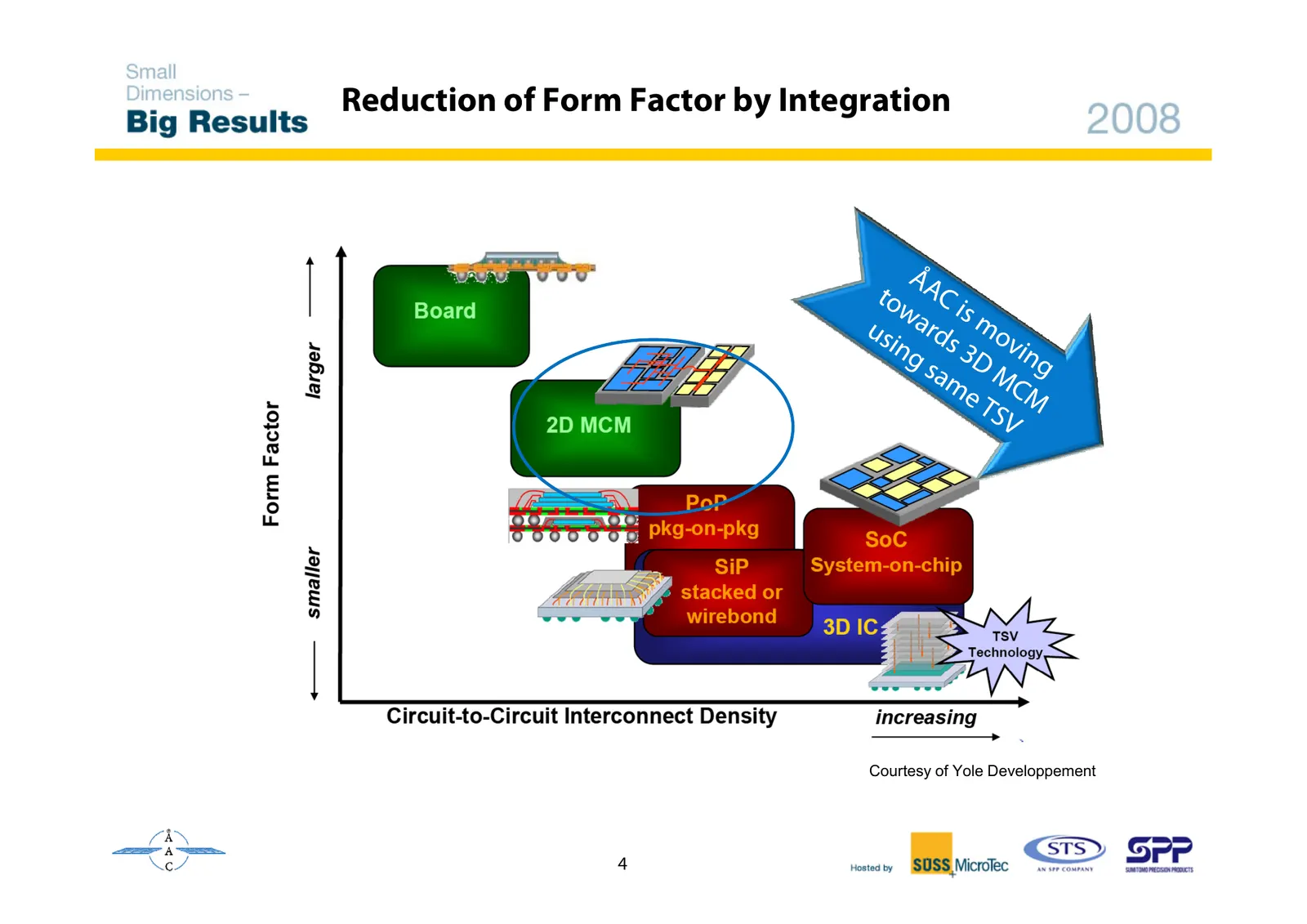
Reduction of Form Factor by Integration Courtesy of Yole Developpement 4
Slide 5: ÅAC position in the world of TSV – Via Size
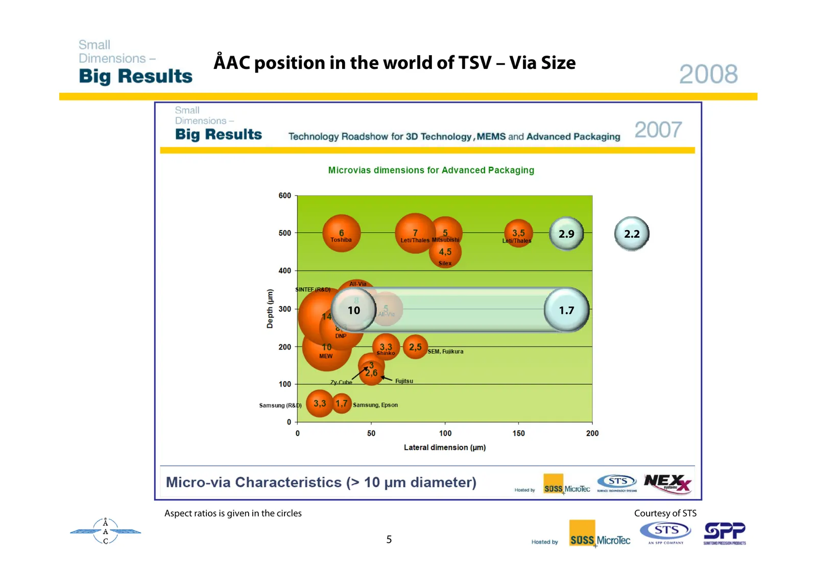
ÅAC position in the world of TSV – Via Size 2.9 2.2 10 1.7 Aspect ratios is given in the circles Courtesy of STS 5
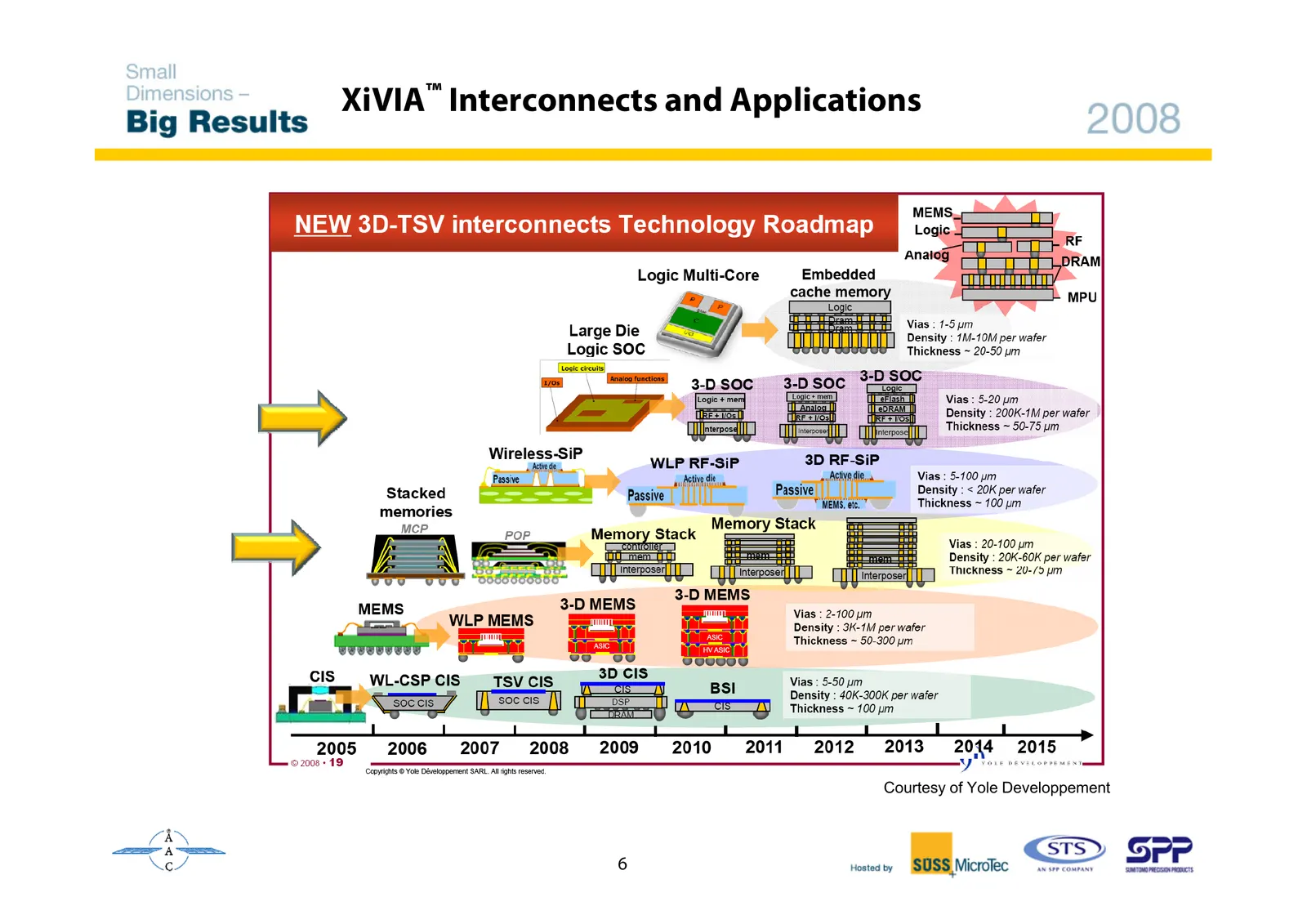
Slide 6: XiVIA Interconnects and Applications
XiVIA™ Interconnects and Applications Courtesy of Yole Developpement 6
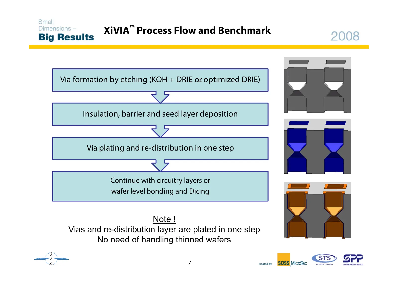
Slide 7: XiVIA Process Flow and Benchmark
XiVIA™ Process Flow and Benchmark Vi formation Via f i byb etching hi (KOH + DRIE or optimized i i d DRIE) Insulation, barrier and seed layer deposition Via plating and re-distribution in one step Continue with circuitry layers or wafer level bonding and Dicing Note ! Vias and re-distribution layer
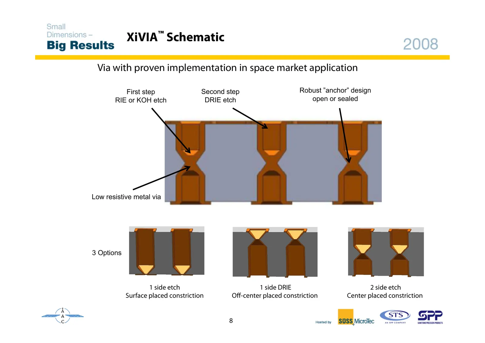
Slide 8: XiVIA Schematic
XiVIA™ Schematic Via with proven implementation in space market application First step Second step Robust ”anchor” design g RIE or KOH etch DRIE etch open or sealed Low resistive metal via 3 Options 1 side etch 1 side DRIE 2 side etch Surface placed constriction Off-center placed constriction Center
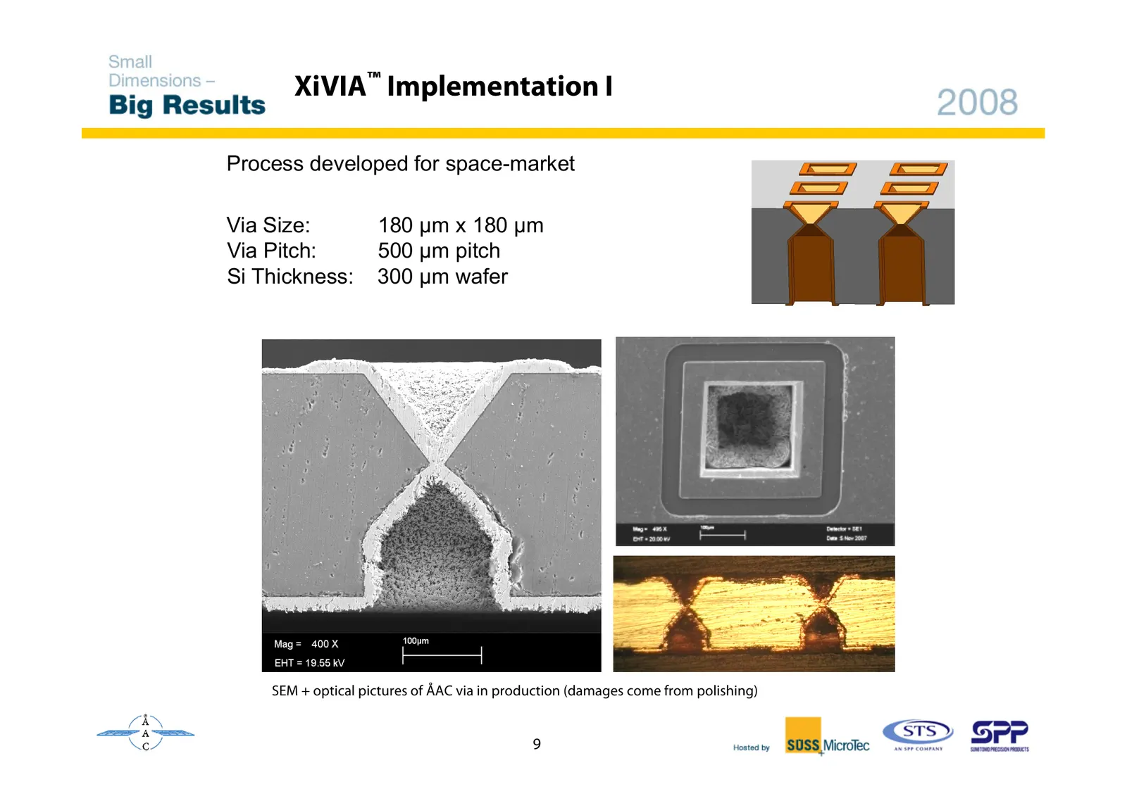
Slide 9: XiVIA Implementation I
XiVIA™ Implementation I Process developed for space-market Via Si Vi Size: 180 µm x 180 µm Via Pitch: 500 µm pitch Si Thickness: 300 µm wafer SEM + optical pictures of ÅAC via in production (damages come from polishing) 9
Slide 10: XiVIA Implementation II
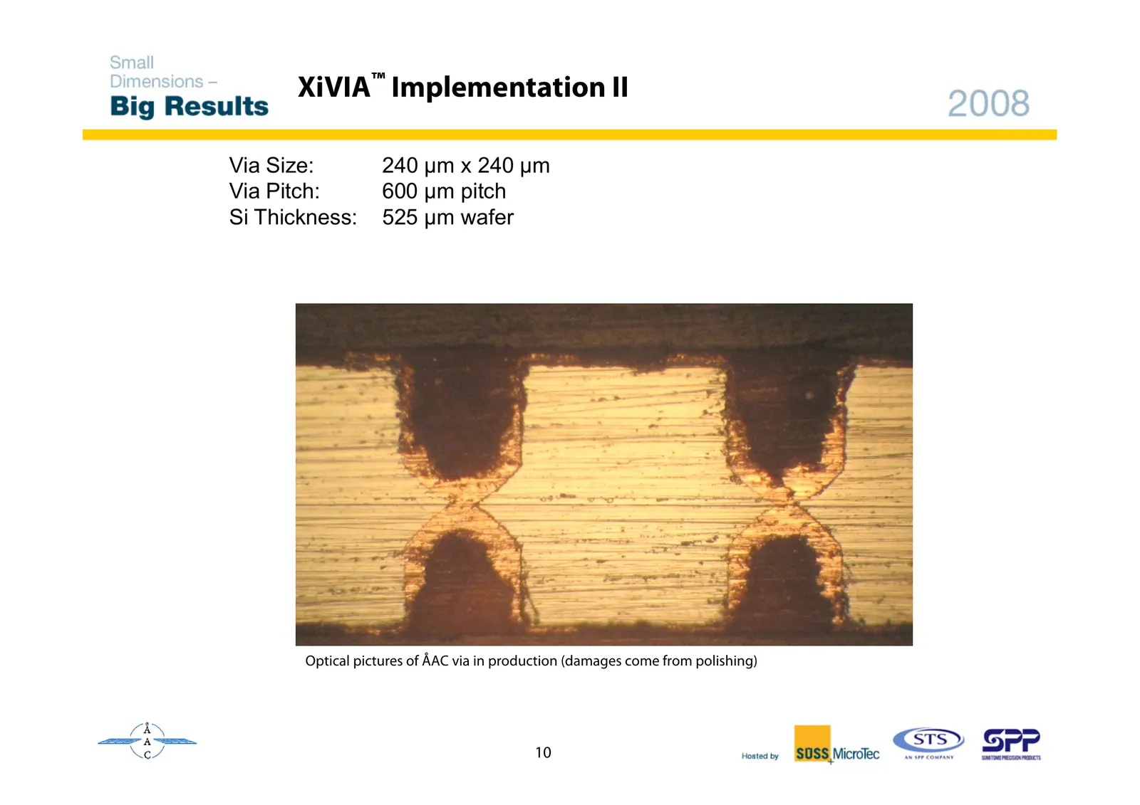
XiVIA™ Implementation II Via Size: 240 µm x 240 µm Via Pitch: 600 µm pitch Si Thickness: 525 µm wafer Optical pictures of ÅAC via in production (damages come from polishing) 10
Slide 11: XiVIA Implementation II
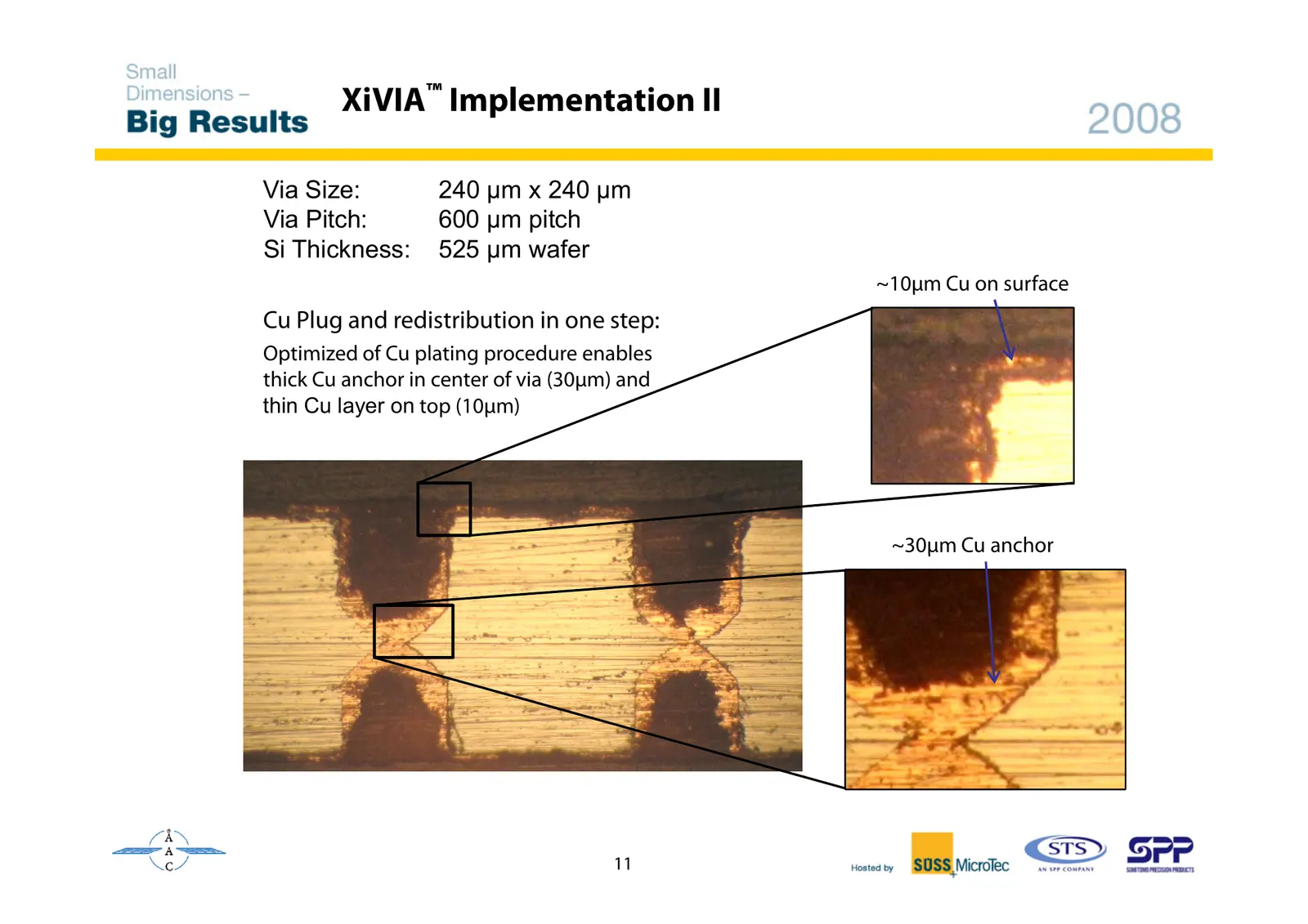
XiVIA™ Implementation II Via Size: 240 µm x 240 µm Via Pitch: 600 µm pitch Si Thickness: 525 µm wafer ~10μm Cu on surface Cu Plug and redistribution in one step: Optimized of Cu plating procedure enables thick Cu anchor in center of via (30μm) and thin Cu layer on top (10μm) ~30μm Cu anchor 11
Slide 12: XiVIA unique TSV features
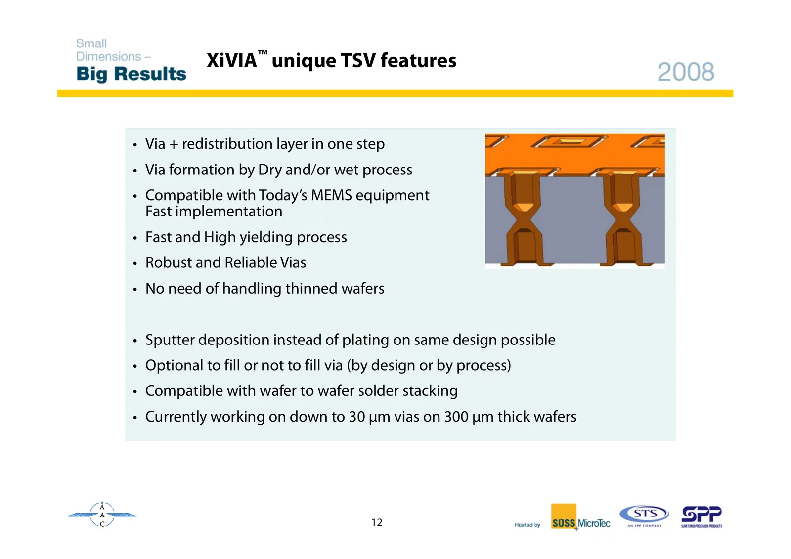
XiVIA™ unique TSV features • Via + redistribution layer y in one step • Via formation by Dry and/or wet process • Compatible with Today’s MEMS equipment Fast implementation • Fast and High yielding process • Robust and Reliable Vias • No need of handling thinned wafers • Sputter deposition instead o
Slide 13: XiVIA Features
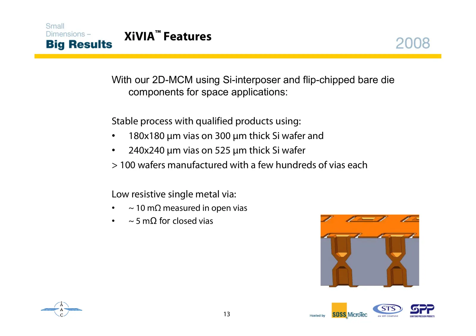
XiVIA™ Features With our 2D-MCM using Si-interposer and flip-chipped bare die components for space applications: Stable process with qualified products using: • 180x180 μm vias on 300 μm thick Si wafer and • 240x240 μm vias on 525 μm thick Si wafer > 100 wafers manufactured with a few hundreds of vi
Slide 14: XiVIA reliability - I
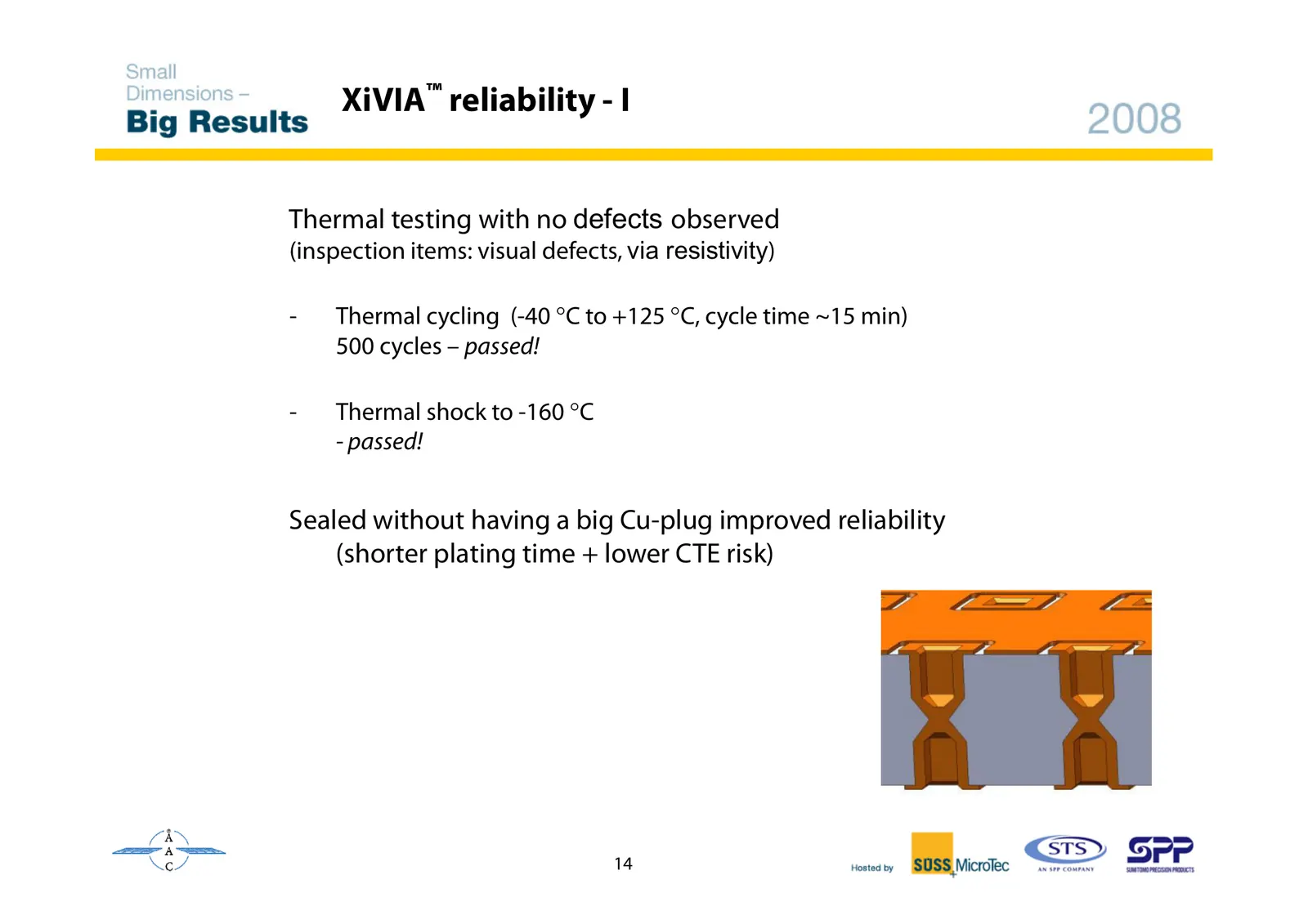
XiVIA™ reliability - I Thermal testing with no defects observed defects via resistivity) (inspection items: visual defects, - Thermal cycling (-40 °C to +125 °C, cycle time ~15 min) 500 cycles y –p passed! - Thermal shock to -160 °C - passed! Sealed without having a big Cu-plug improved reliability
Slide 15: XiVIA reliability - II
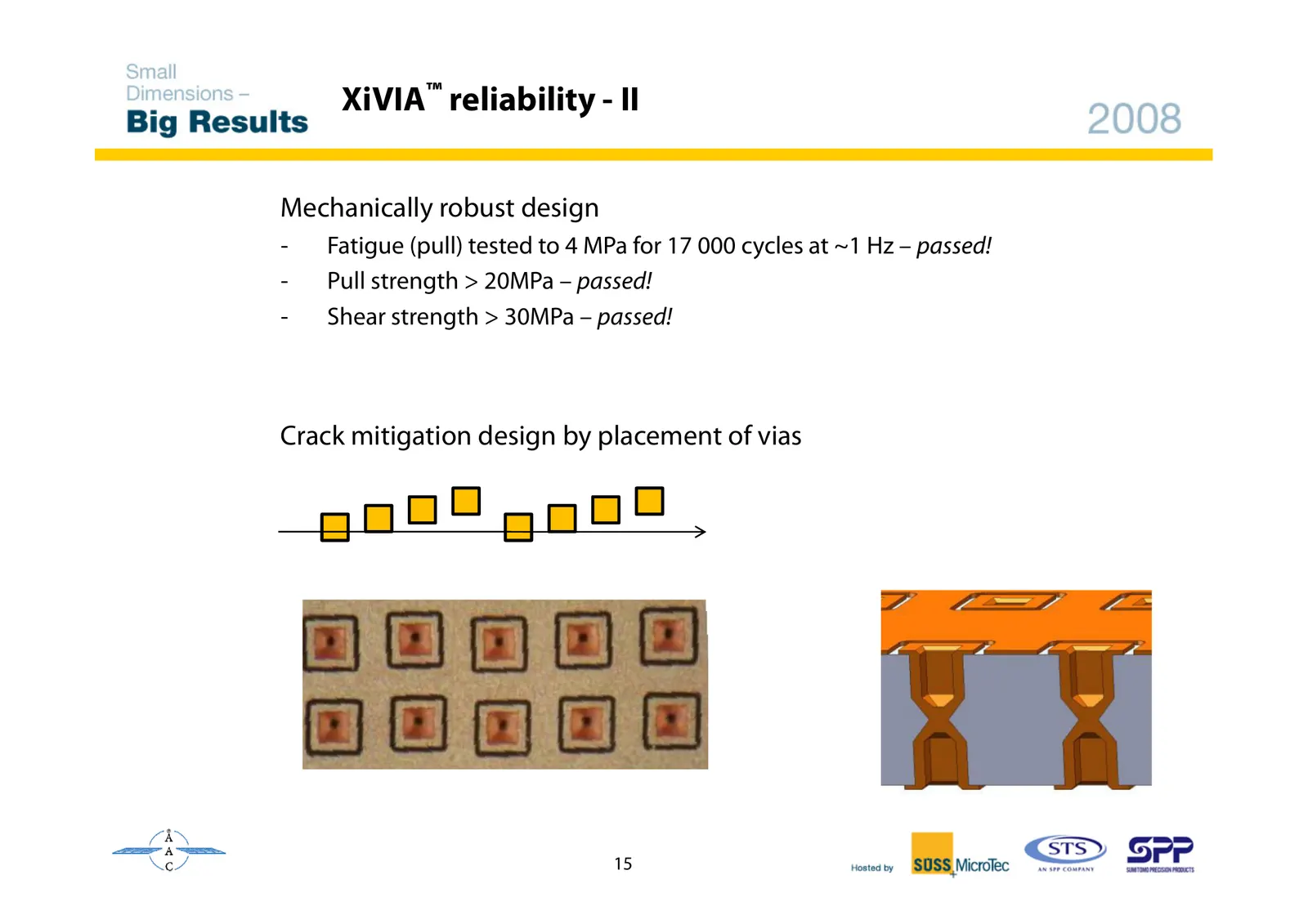
XiVIA™ reliability - II Mechanically robust design - Fatigue (pull) tested to 4 MPa for 17 000 cycles at ~1 1 Hz – passed! - Pull strength > 20MPa – passed! - Shear strength > 30MPa – passed! Crack mitigation design by placement of vias 15
Slide 16: XiVIA in Inductor, interposer and SiP
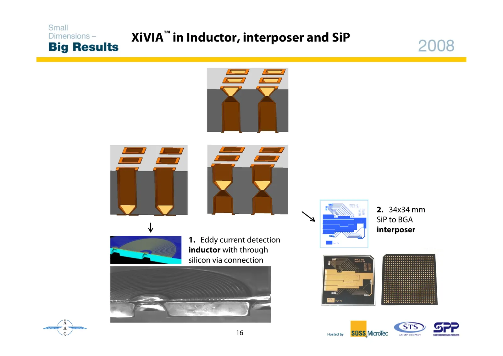
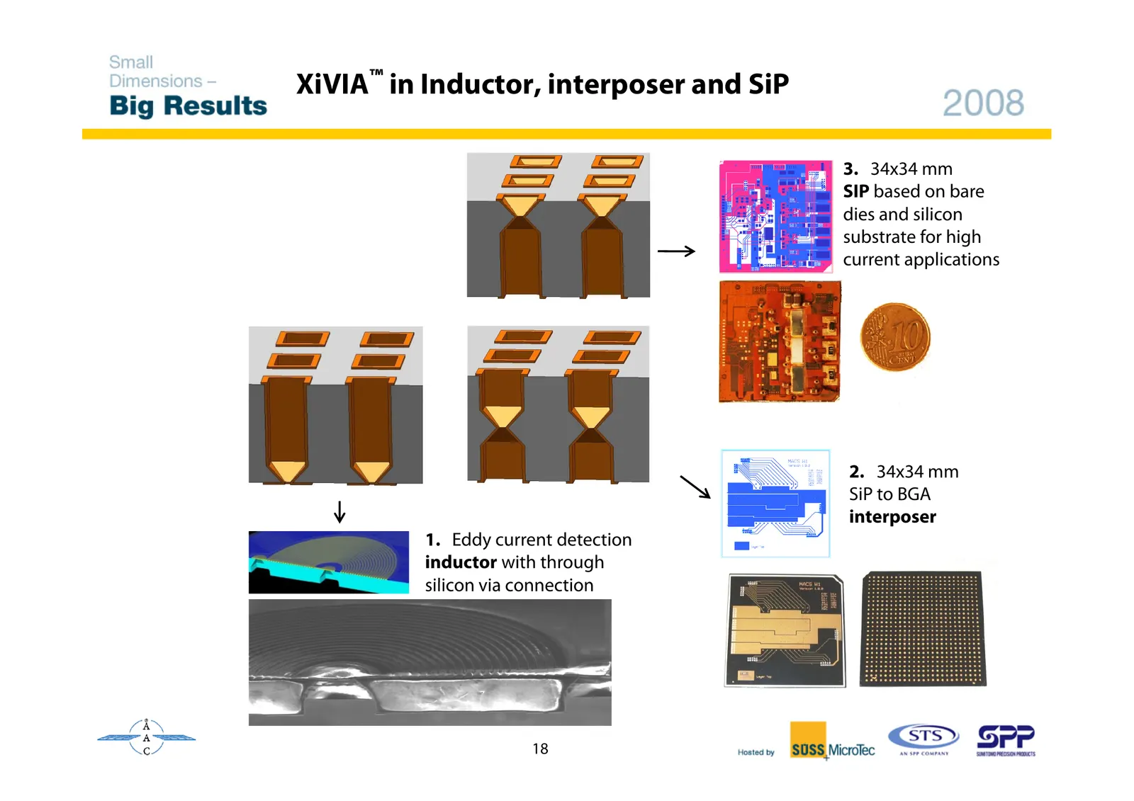
XiVIA™ in Inductor, interposer and SiP 2. 34x34 mm SiP to BGA interposer 1. Eddy current detection inductor with through silicon via ia connection 16
Slide 17: XiVIA in Inductor, interposer and SiP
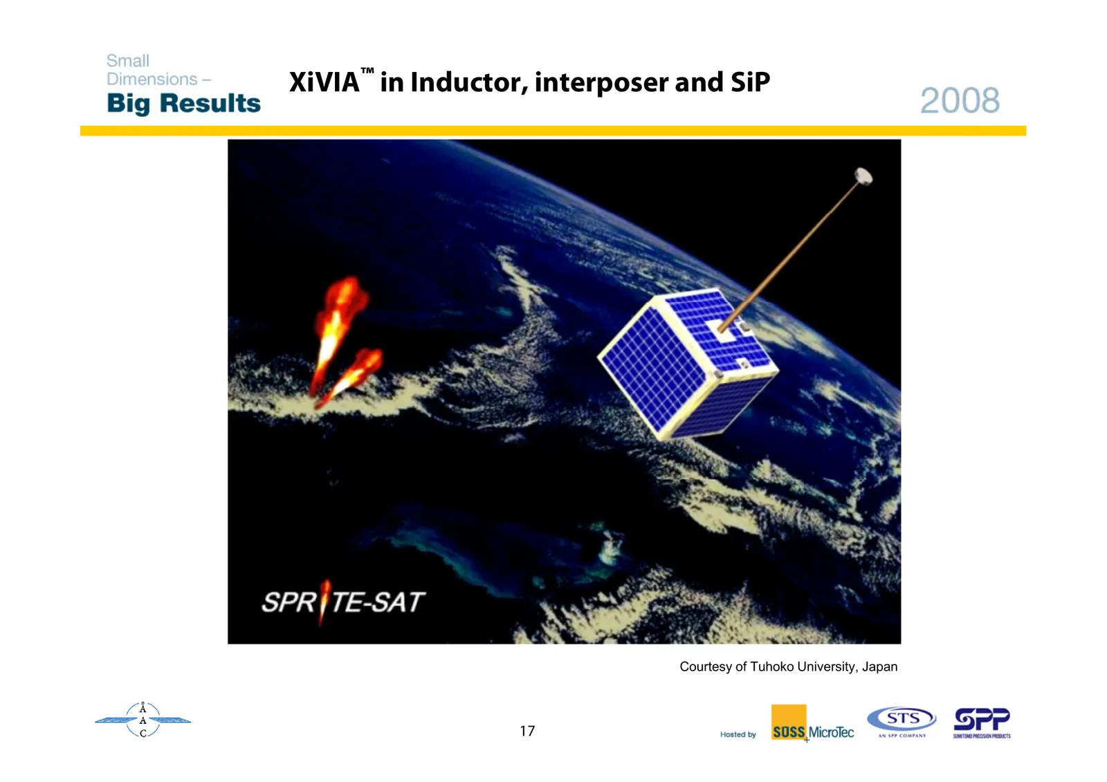
XiVIA™ in Inductor, interposer and SiP Courtesy of Tuhoko University, Japan 17
Slide 18: XiVIA in Inductor, interposer and SiP
XiVIA™ in Inductor, interposer and SiP 3. 34x34 mm SIP based on bare dies and silicon substrate for high current applications 2. 34x34 mm SiP to BGA interposer 1. Eddy current detection inductor with through silicon via ia connection 18
Slide 19: XiVIA in Inductor, interposer and SiP
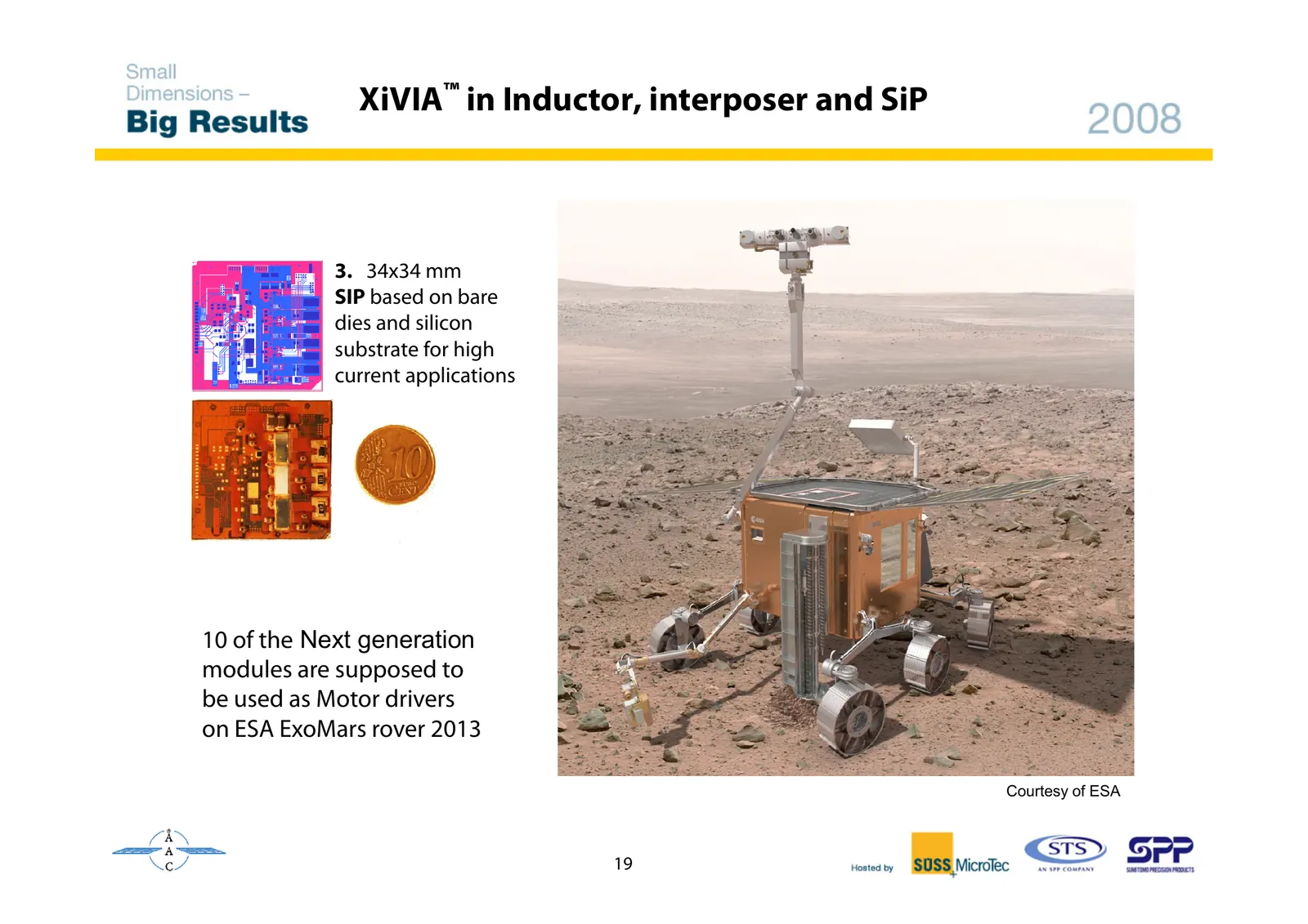
XiVIA™ in Inductor, interposer and SiP 3. 34x34 mm SIP based on bare dies and silicon substrate for high g current applications 10 of the Next generation modules are supposed to be used as Motor drivers on ESA ExoMars rover 2013 Courtesy of ESA 19
Slide 20: MCM/SIP with BGA interposer
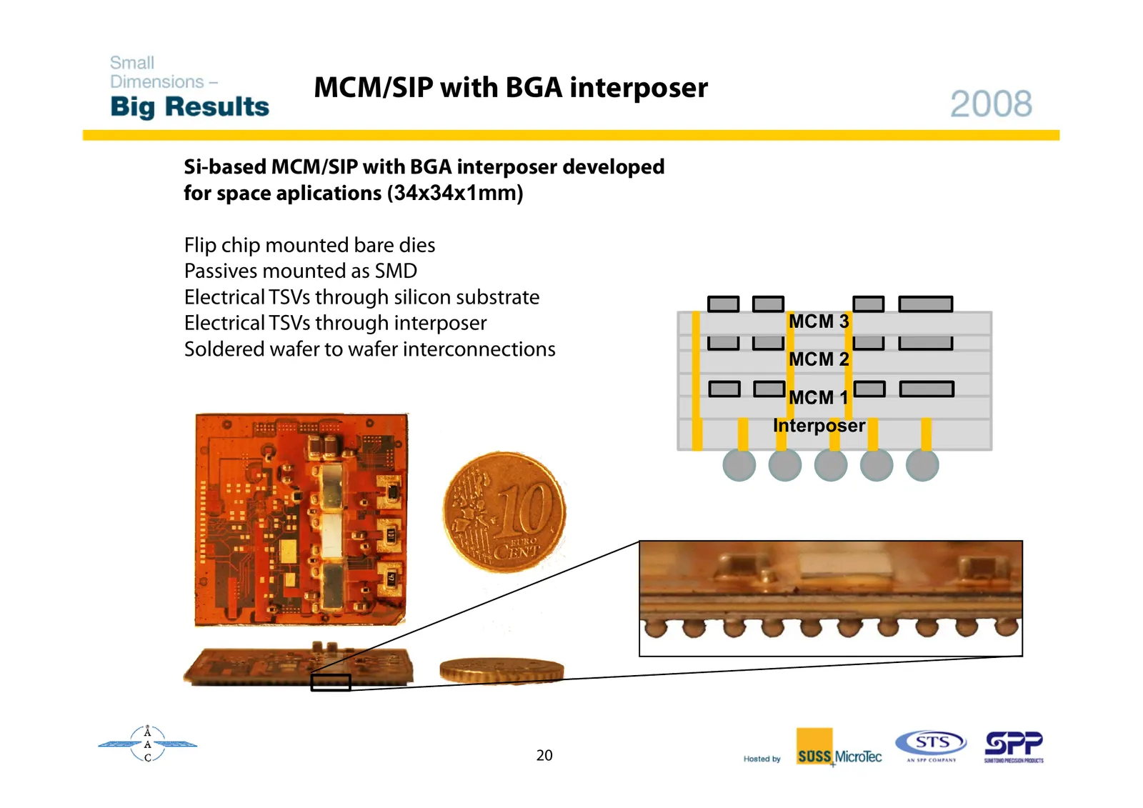
MCM/SIP with BGA interposer Si-based MCM/SIP with BGA interposer developed for space aplications (34x34x1mm) Flip chip mounted bare dies Passives mounted as SMD Electrical TSVs through silicon substrate Electrical TSVs through interposer MCM 3 Soldered wafer to wafer interconnections MCM 2 MCM 1 Int
Slide 21: MCM/SIP with BGA interposer X-ray
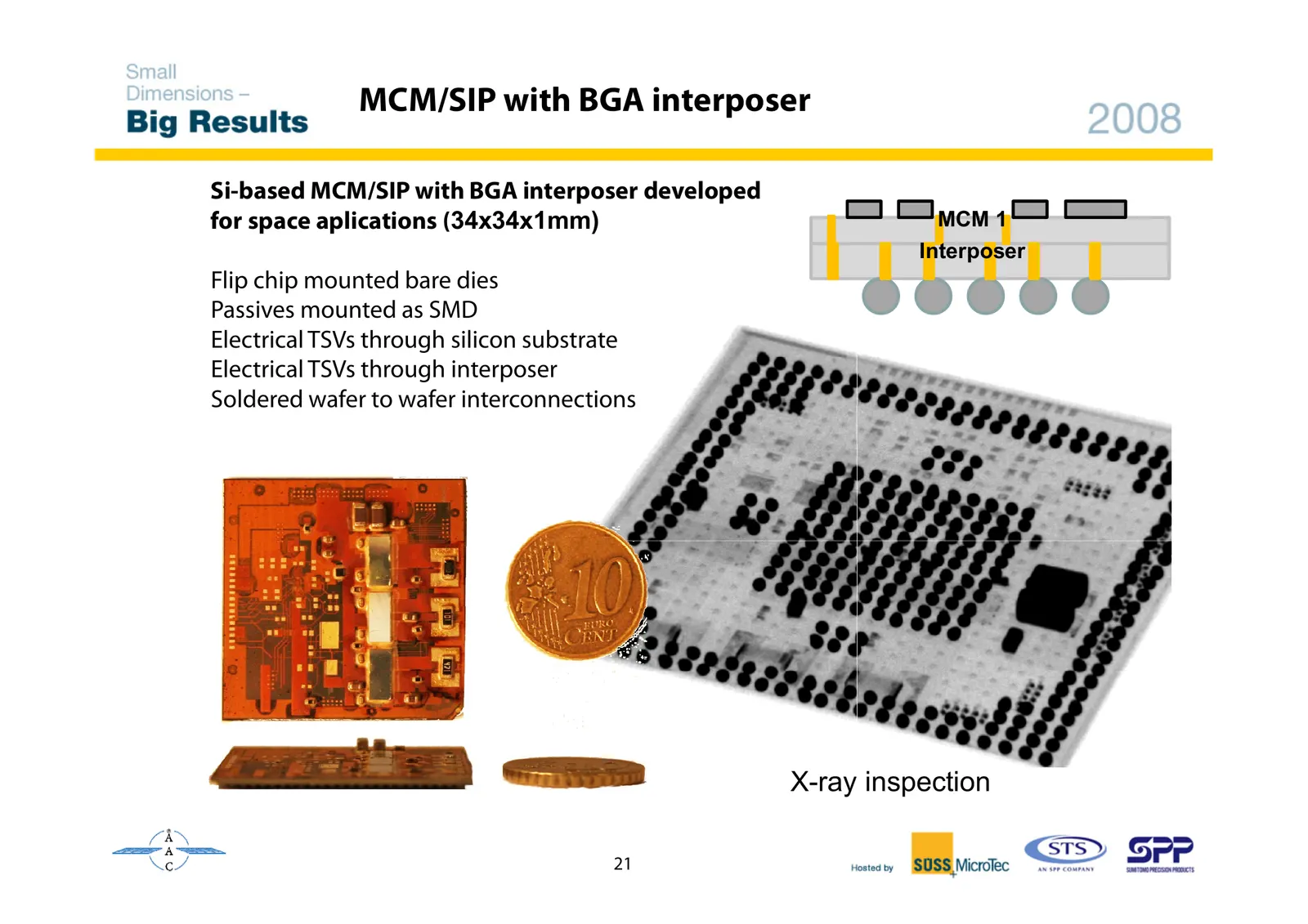
MCM/SIP with BGA interposer Si-based MCM/SIP with BGA interposer developed for space aplications (34x34x1mm) MCM 1 Interposer Flip chip mounted bare dies Passives mounted as SMD Electrical TSVs through silicon substrate Electrical TSVs through interposer Soldered wafer to wafer interconnections X X-
Slide 22: XiVIA Potential applications
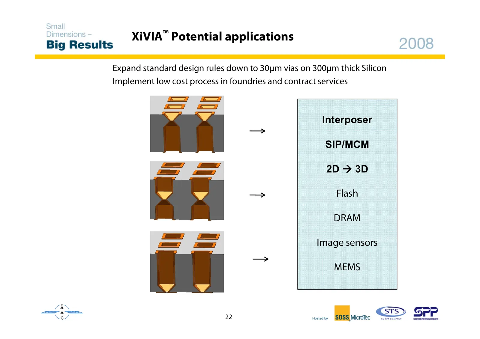
XiVIA™ Potential applications Expand standard design rules down to 30μm vias on 300μm thick Silicon Implement low cost process in foundries and contract services Interposer SIP/MCM 2D Æ 3D Flash DRAM Image g sensors MEMS 22
Slide 23: XiVIA design solves process issues
XiVIA™ design solves process issues Unique constriction design solves main process issues: • Improved uniformity and reduced void formation during Cu plating • Improved step coverage and side wall coverage at center of wafer during sputtering • Improved and simplified end detection for via etching •
Slide 24: XiVIA Summary
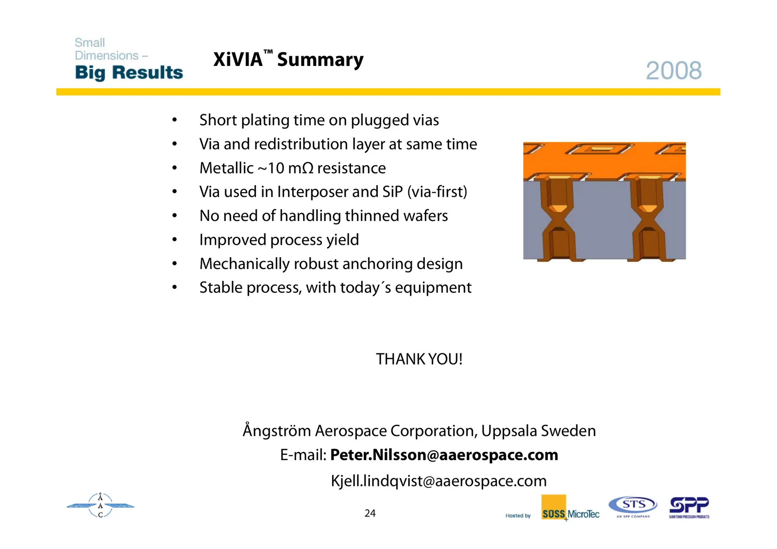
XiVIA™ Summary • Short plating time on plugged vias • Via and redistribution layer y at same time • Metallic ~10 mΩ resistance • Via used in Interposer and SiP (via-first) • N need No d off handling h dli thinned thi d wafers f • Improved process yield • Mechanically robust anchoring design • Stable
Source: Internet Archive copy of aacmicrotec.com