SUSS MicroTec SE · XETR:SMHN
SUSS MicroTec — Investor Day (September 2020)
7 slides from SUSS MicroTec's investor day presentation, Sep 24, 2020
Slide 1: Capital Markets Day 2020: Insights Photomask Equipment
CAPITAL MARKETS DAY 2020 INSIGHTS PHOTOMASK EQUIPMENT September 24, 2020 Yuta Nagai, Business Unit Manager Photomask Equipment
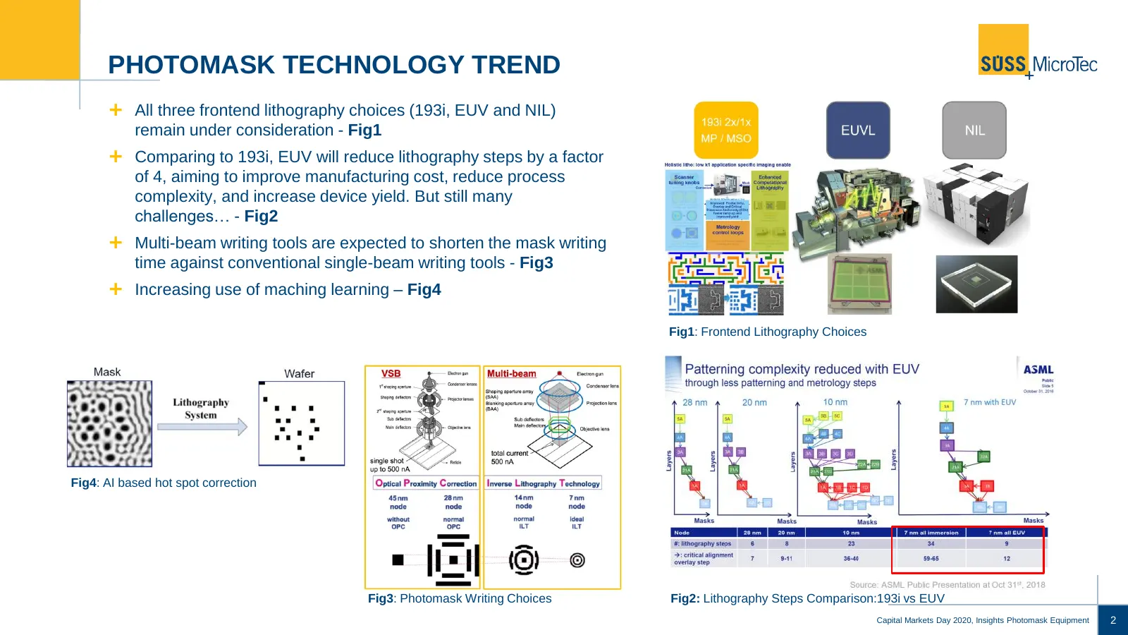
Slide 2: Photomask Technology Trend
PHOTOMASK TECHNOLOGY TREND All three frontend lithography choices (193i, EUV and NIL) remain under consideration - Fig1 Comparing to 193i, EUV will reduce lithography steps by a factor of 4, aiming to improve manufacturing cost, reduce process complexity, and increase device yield. But still man
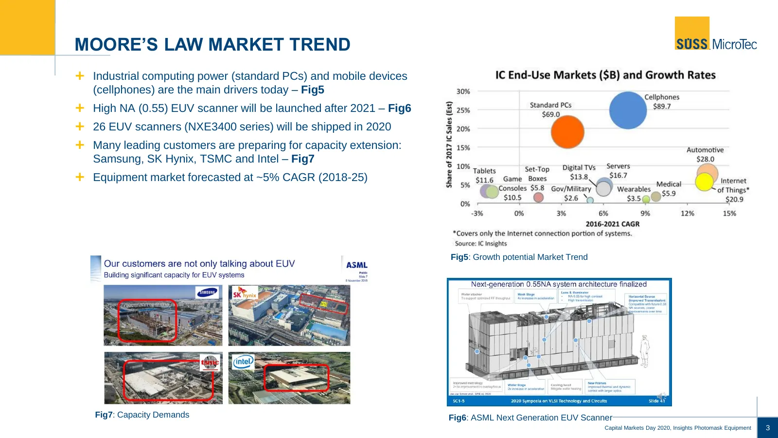
Slide 3: Moore's Law Market Trend
MOORE’S LAW MARKET TREND Industrial computing power (standard PCs) and mobile devices (cellphones) are the main drivers today – Fig5 High NA (0.55) EUV scanner will be launched after 2021 – Fig6 26 EUV scanners (NXE3400 series) will be shipped in 2020 Many leading customers are preparing for
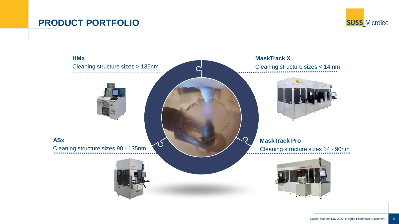
Slide 4: Product Portfolio
PRODUCT PORTFOLIO HMx MaskTrack X Cleaning structure sizes > 135nm Cleaning structure sizes < 14 nm ASx MaskTrack Pro Cleaning structure sizes 90 - 135nm Cleaning structure sizes 14 - 90nm Capital Markets Day 2020, Insights Photomask Equipment 4
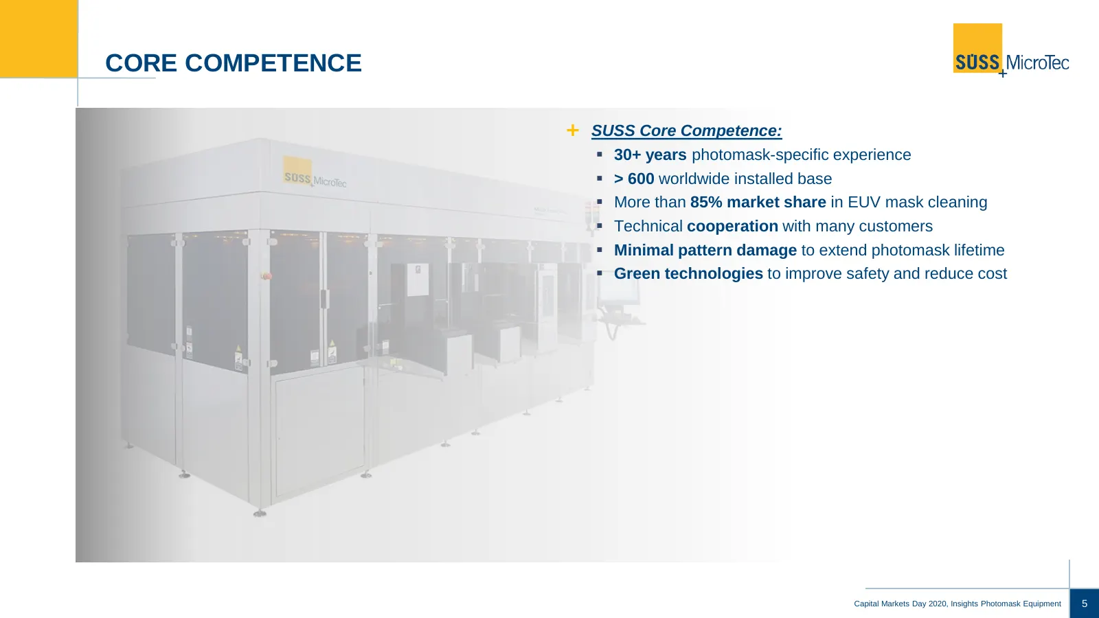
Slide 5: Core Competence
CORE COMPETENCE SUSS Core Competence: 30+ years photomask-specific experience > 600 worldwide installed base More than 85% market share in EUV mask cleaning Technical cooperation with many customers Minimal pattern damage to extend photomask lifetime Green technologies to improve safet
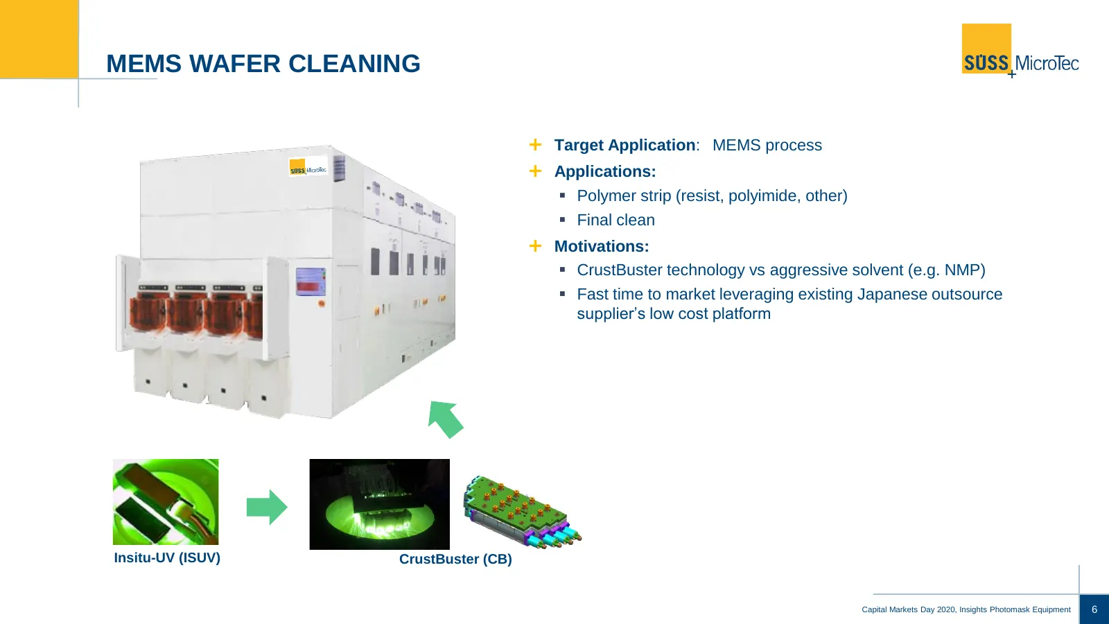
Slide 6: MEMS Wafer Cleaning
MEMS WAFER CLEANING Target Application: MEMS process Applications: Polymer strip (resist, polyimide, other) Final clean Motivations: CrustBuster technology vs aggressive solvent (e.g. NMP) Fast time to market leveraging existing Japanese outsource supplier’s low cost platform Insitu-UV

Slide 7: SÜSS MicroTec SE contact details
SÜSS MicroTec SE | Schleissheimer Str. 90 | 85748 Garching | www.suss.com
Source: Internet Archive copy of suss.com
More decks from SUSS MicroTec SE
 9M 2026 Earnings Presentation23 slides · Nov 5, 2026
 Investor Presentation (October 2026)41 slides · October 2026
 H1 2026 Earnings Presentation24 slides · Aug 6, 2026
 Q1 2026 Earnings Presentation19 slides · May 7, 2026
 FY2025 Earnings Presentation26 slides · Mar 30, 2026
 Investor Presentation (March 2026)42 slides · Mar 1, 2026